RM0367 Rev 7 275/1043
RM0367 Direct memory access controller (DMA)
288
Addressing AHB peripherals not supporting byte/half-word write transfers
When the DMA controller initiates an AHB byte or half-word write transfer, the data are
duplicated on the unused lanes of the AHB master 32-bit data bus (HWDATA[31:0]).
When the AHB slave peripheral does not support byte or half-word write transfers and does
not generate any error, the DMA controller writes the 32 HWDATA bits as shown in the two
examples below:
• To write the half-word 0xABCD, the DMA controller sets the HWDATA bus to
0xABCDABCD with a half-word data size (HSIZE = HalfWord in AHB master bus).
• To write the byte 0xAB, the DMA controller sets the HWDATA bus to 0xABABABAB
with a byte data size (HSIZE = Byte in the AHB master bus).
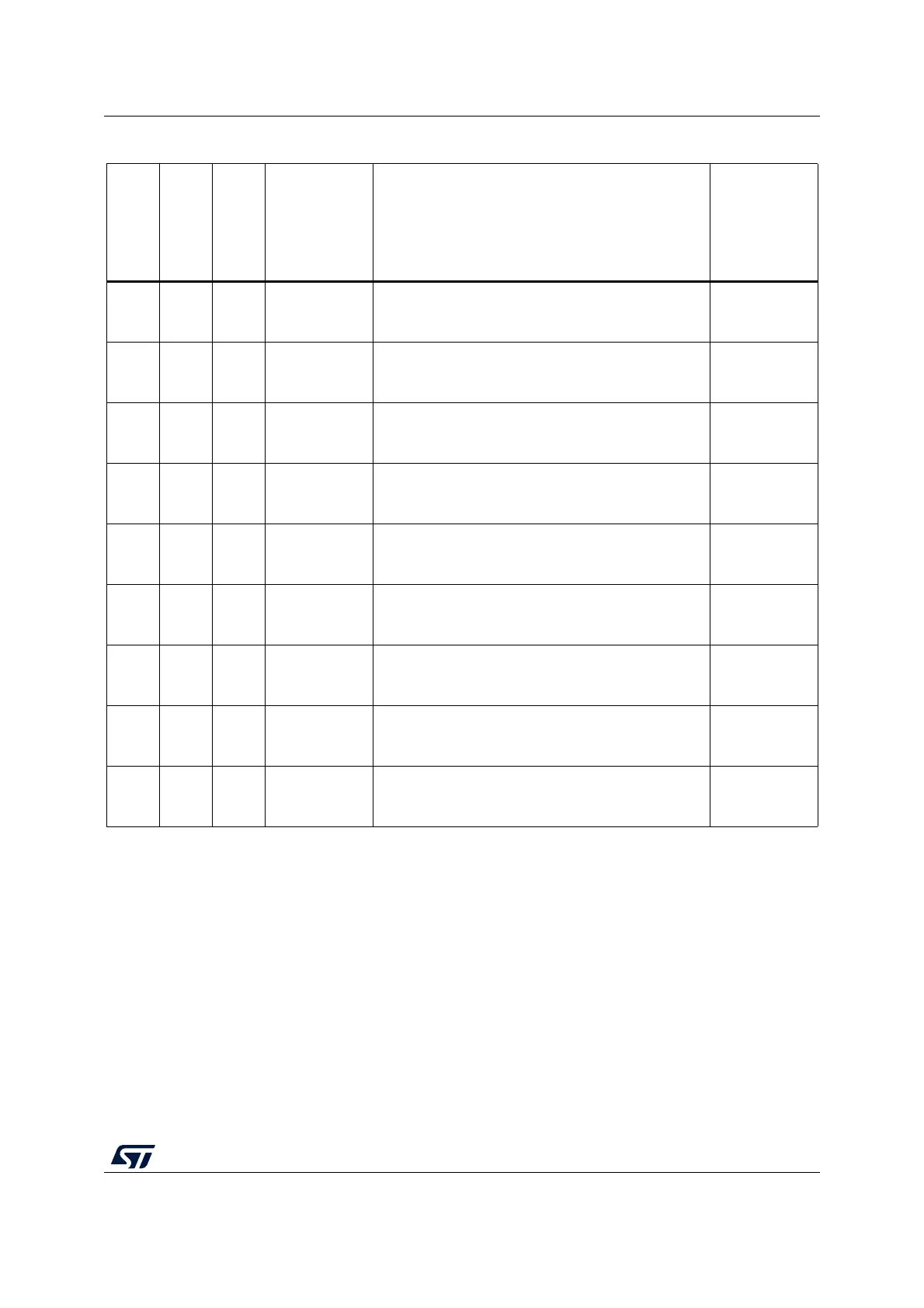
Table 52. Programmable data width and endian behavior (when PINC=MINC=1)
Source
port
width
(MSIZE
if
DIR = 1,
else
PSIZE)
Destinat
ion port
width
(PSIZE
if
DIR = 1,
else
MSIZE)
Number
of data
items to
transfer
(NDT)
Source content:
address / data
(DMA_CMARx if
DIR = 1, else
DMA_CPARx)
DMA transfers
Destination
content:
address / data
(DMA_CPARx if
DIR = 1, else
DMA_CMARx)
884
@0x0 / B0
@0x1 / B1
@0x2 / B2
@0x3 / B3
1: read B0[7:0] @0x0 then write B0[7:0] @0x0
2: read B1[7:0] @0x1 then write B1[7:0] @0x1
3: read B2[7:0] @0x2 then write B2[7:0] @0x2
4: read B3[7:0] @0x3 then write B3[7:0] @0x3
@0x0 / B0
@0x1 / B1
@0x2 / B2
@0x3 / B3
8164
@0x0 / B0
@0x1 / B1
@0x2 / B2
@0x3 / B3
1: read B0[7:0] @0x0 then write 00B0[15:0] @0x0
2: read B1[7:0] @0x1 then write 00B1[15:0] @0x2
3: read B2[7:0] @0x2 then write 00B2[15:0] @0x4
4: read B3[7:0] @0x3 then write 00B3[15:0] @0x6
@0x0 / 00B0
@0x2 / 00B1
@0x4 / 00B2
@0x6 / 00B3
8324
@0x0 / B0
@0x1 / B1
@0x2 / B2
@0x3 / B3
1: read B0[7:0] @0x0 then write 000000B0[31:0] @0x0
2: read B1[7:0] @0x1 then write 000000B1[31:0] @0x4
3: read B2[7:0] @0x2 then write 000000B2[31:0] @0x8
4: read B3[7:0] @0x3 then write 000000B3[31:0] @0xC
@0x0 / 000000B0
@0x4 / 000000B1
@0x8 / 000000B2
@0xC / 000000B3
16 8 4
@0x0 / B1B0
@0x2 / B3B2
@0x4 / B5B4
@0x6 / B7B6
1: read B1B0[15:0] @0x0 then write B0[7:0] @0x0
2: read B3B2[15:0] @0x2 then write B2[7:0] @0x1
3: read B5B4[15:0] @0x4 then write B4[7:0] @0x2
4: read B7B6[15:0] @0x6 then write B6[7:0] @0x3
@0x0 / B0
@0x1 / B2
@0x2 / B4
@0x3 / B6
16 16 4
@0x0 / B1B0
@0x2 / B3B2
@0x4 / B5B4
@0x6 / B7B6
1: read B1B0[15:0] @0x0 then write B1B0[15:0] @0x0
2: read B3B2[15:0] @0x2 then write B3B2[15:0] @0x2
3: read B5B4[15:0] @0x4 then write B5B4[15:0] @0x4
4: read B7B6[15:0] @0x6 then write B7B6[15:0] @0x6
@0x0 / B1B0
@0x2 / B3B2
@0x4 / B5B4
@0x6 / B7B6
16 32 4
@0x0 / B1B0
@0x2 / B3B2
@0x4 / B5B4
@0x6 / B7B6
1: read B1B0[15:0] @0x0 then write 0000B1B0[31:0] @0x0
2: read B3B2[15:0] @0x2 then write 0000B3B2[31:0] @0x4
3: read B5B4[15:0] @0x4 then write 0000B5B4[31:0] @0x8
4: read B7B6[15:0] @0x6 then write 0000B7B6[31:0] @0xC
@0x0 / 0000B1B0
@0x4 / 0000B3B2
@0x8 / 0000B5B4
@0xC / 0000B7B6
32 8 4
@0x0 / B3B2B1B0
@0x4 / B7B6B5B4
@0x8 / BBBAB9B8
@0xC / BFBEBDBC
1: read B3B2B1B0[31:0] @0x0 then write B0[7:0] @0x0
2: read B7B6B5B4[31:0] @0x4 then write B4[7:0] @0x1
3: read BBBAB9B8[31:0] @0x8 then write B8[7:0] @0x2
4: read BFBEBDBC[31:0] @0xC then write BC[7:0] @0x3
@0x0 / B0
@0x1 / B4
@0x2 / B8
@0x3 / BC
32 16 4
@0x0 / B3B2B1B0
@0x4 / B7B6B5B4
@0x8 / BBBAB9B8
@0xC / BFBEBDBC
1: read B3B2B1B0[31:0] @0x0 then write B1B0[15:0] @0x0
2: read B7B6B5B4[31:0] @0x4 then write B5B4[15:0] @0x2
3: read BBBAB9B8[31:0] @0x8 then write B9B8[15:0] @0x4
4: read BFBEBDBC[31:0] @0xC then write BDBC[15:0] @0x6
@0x0 / B1B0
@0x2 / B5B4
@0x4 / B9B8
@0x6 / BDBC
32 32 4
@0x0 / B3B2B1B0
@0x4 / B7B6B5B4
@0x8 / BBBAB9B8
@0xC / BFBEBDBC
1: read B3B2B1B0[31:0] @0x0 then write B3B2B1B0[31:0] @0x0
2: read B7B6B5B4[31:0] @0x4 then write B7B6B5B4[31:0] @0x4
3: read BBBAB9B8[31:0] @0x8 then write BBBAB9B8[31:0] @0x8
4: read BFBEBDBC[31:0] @0xC then write BFBEBDBC[31:0] @0xC
@0x0 / B3B2B1B0
@0x4 / B7B6B5B4
@0x8 / BBBAB9B8
@0xC / BFBEBDBC
 Loading...


