Liquid crystal display controller (LCD) RM0367
400/1043 RM0367 Rev 7
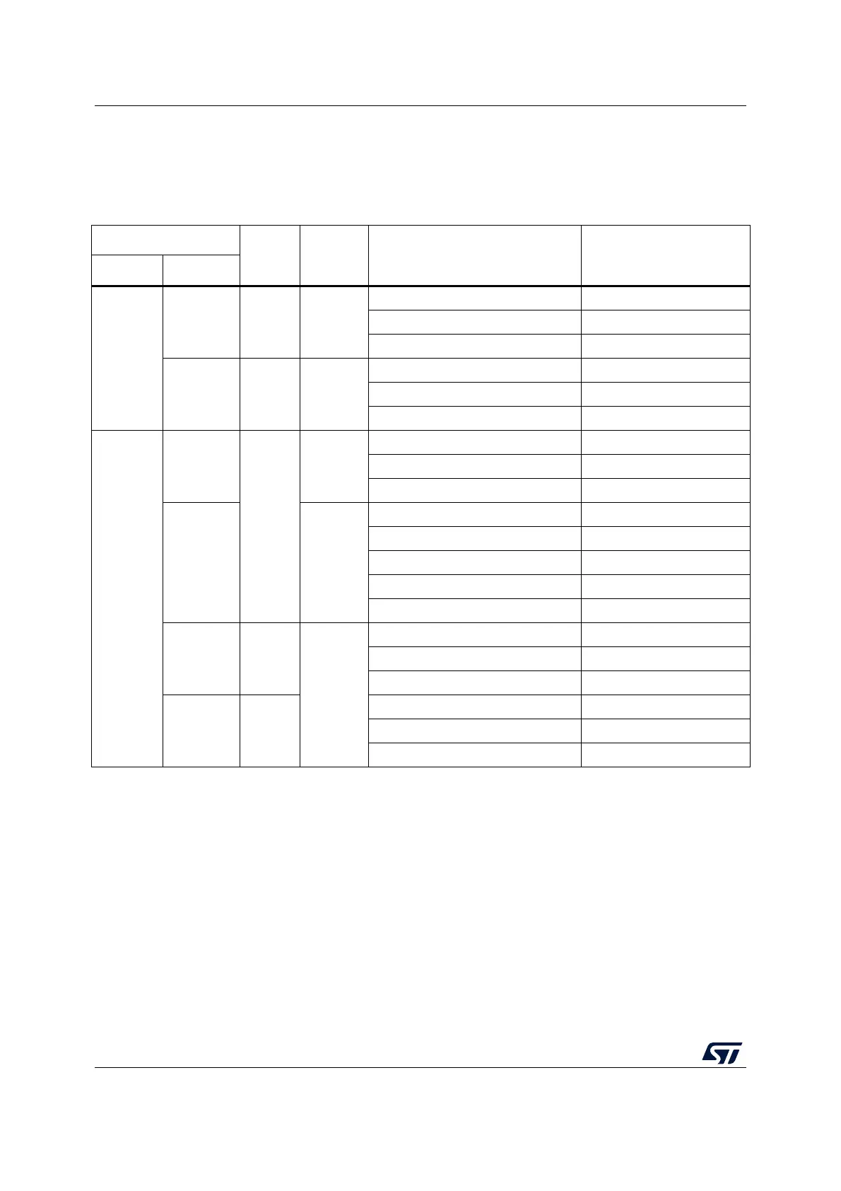
Summary of COM and SEG functions versus duty and remap
All the possible ways of multiplexing the COM and SEG functions are described in Table 77.
Figure 77 gives examples showing the signal connections to the external pins.
Table 77. Remapping capability
(1)
Configuration bits QFP64/
BGA64
(2)
BGA100/
LQFP100
Output pin Function
DUTY MUX_SEG
1/8
0/1 - 48x8
SEG[51:48]/SEG[31:28]/COM[7:4] COM[7:4]
COM[3:0] COM[3:0]
SEG[47:0] SEG[47:0]
0/1 28x8 -
SEG[51:48]/SEG[31:28]/COM[7:4] COM[7:4]
COM[3:0] COM[3:0]
SEG[27:0] SEG[27:0]
1/4
0
-
52x4
COM[3:0] COM[3:0]
SEG[51:48]/SEG[31:28]/COM[7:4] SEG[51:48]
SEG[47:0] SEG[47:0]
148x4
COM[3:0] COM[3:0]
SEG[51:48]/SEG[31:28]/COM[7:4] SEG[31:28]
SEG[47:32] SEG[47:32]
SEG[31:28] not used
SEG[27:0] SEG[27:0]
0 28x4
-
COM[3:0] COM[3:0]
SEG[51:48]/SEG[31:28]/COM[7:4] not used
SEG[27:0] SEG[27:0]
1 32x4
COM[3:0] COM[3:0]
SEG[51:48]/SEG[31:28]/COM[7:4] SEG[31:28]
SEG[27:0] SEG[27:0]