RM0367 Rev 7 177/1043
RM0367 Reset and clock control (RCC)
225
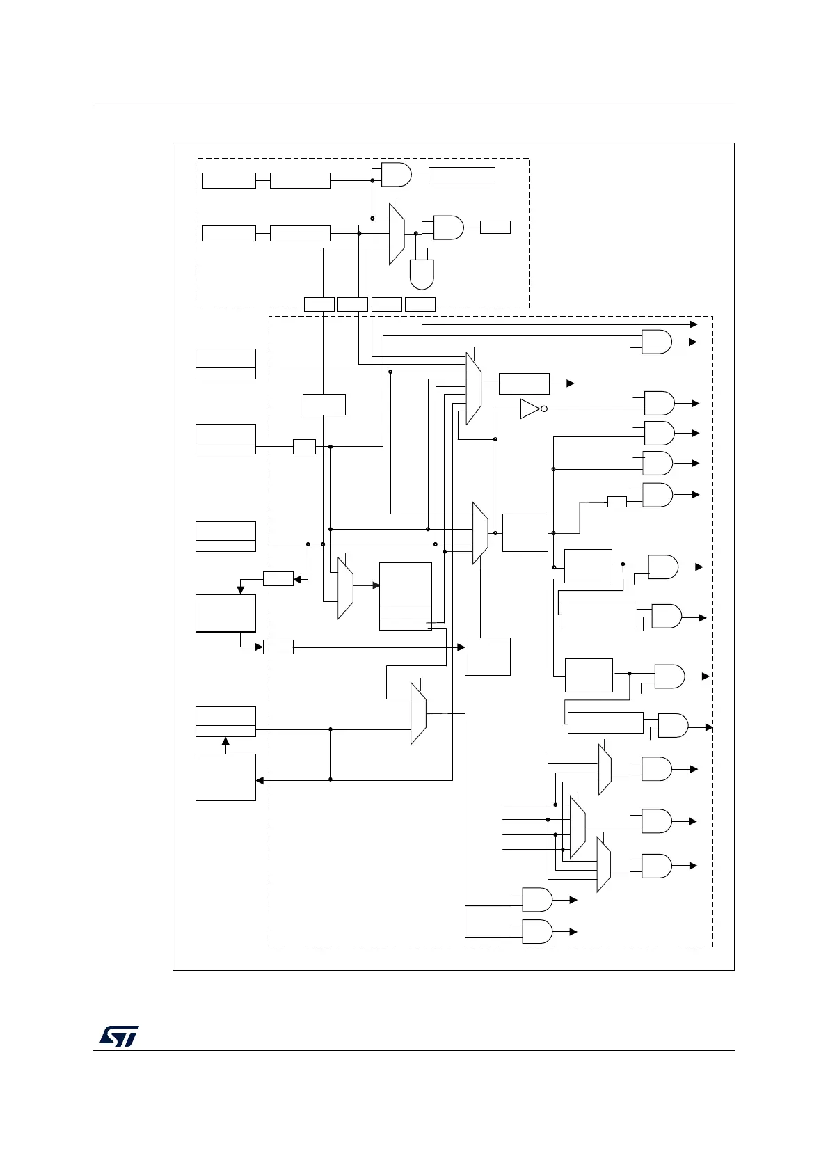
Figure 17. Clock tree
1. For full details about the internal and external clock source characteristics, please refer to the “Electrical
characteristics” section in your device datasheet.
MS32912V2
Legend:
HSE = High-speed external clock signal
HSI = High-speed internal clock signal
LSI = Low-speed internal clock signal
LSE = Low-speed external clock signal
MSI = Multispeed internal clock signal
Watchdog LS
LSI RC
LSE OSC
RTC
LSI tempo
@V33
/ 1,2,4,8,16
HSI16 RC
Level shifters
HSE OSC
Level shifters
RC 48MHz
Level shifters
LSU
1 MHz Clock
Detector
LSD
Clock
Recovery
System
/ 8
LSE tempo
MSI RC
Level shifters
/ 2,4,8,16
/ 2,3,4
Level shifters
PLL
X
3,4,6,8,12,16,
24,32,48
APB1
PRESC
/ 1,2,4,8,16
AHB
PRESC
/ 1,2,…, 512
Clock
Source
Control
usb_en
@V33
@V33
@V33
@V33
@V33
@V18
@V18
@V18
@V18
@V18
rng_en
48MHz
USBCLK
48MHz RNG
I2C1CLK
LPUART/
UARTCLK
LPTIMCLK
LSE
HSI16
SYSCLK
PCLK
LSI
Peripheral
clock enable
PCLK1 to APB1
peripherals
not (sleep or
deepsleep)
not (sleep or
deepsleep)
not deepsleep
not deepsleep
HCLK
SysTick
Timer
CK_PWR
FCLK
PLLCLK
HSE
HSI16
MSI
LSE
LSI
Dedicated 48MHz PLL output
HSE present or not
@V33
@V
DDCORE
ck_rchs
/ 1,4
HSI16
HSI48
MSI
1 MHz
ck_pllin
Enable Watchdog
RTC2 enable
LCD enable
ADC enable
ADCCLK
LCDCLK
LSU LSD LSD
MCO
MCOSEL
PLLSRC
HSI48MSEL
RTCSEL
System
Clock
32 MHz
max.
If (APB1 presc=1) x1
else x2)
to TIMx
Peripheral
clock enable
Peripheral
clock enable
Peripheral
clock enable
APB2
PRESC
/ 1,2,4,8,16
Peripheral
clock enable
PCLK2 to APB2
peripherals
32 MHz
max.
If (APB2 presc=1) x1
else x2)
to TIMx
Peripheral
clock enable
LSD
4 MHz
 Loading...


