RM0367 Rev 7 883/1043
RM0367 Serial peripheral interface/ inter-IC sound (SPI/I2S)
922
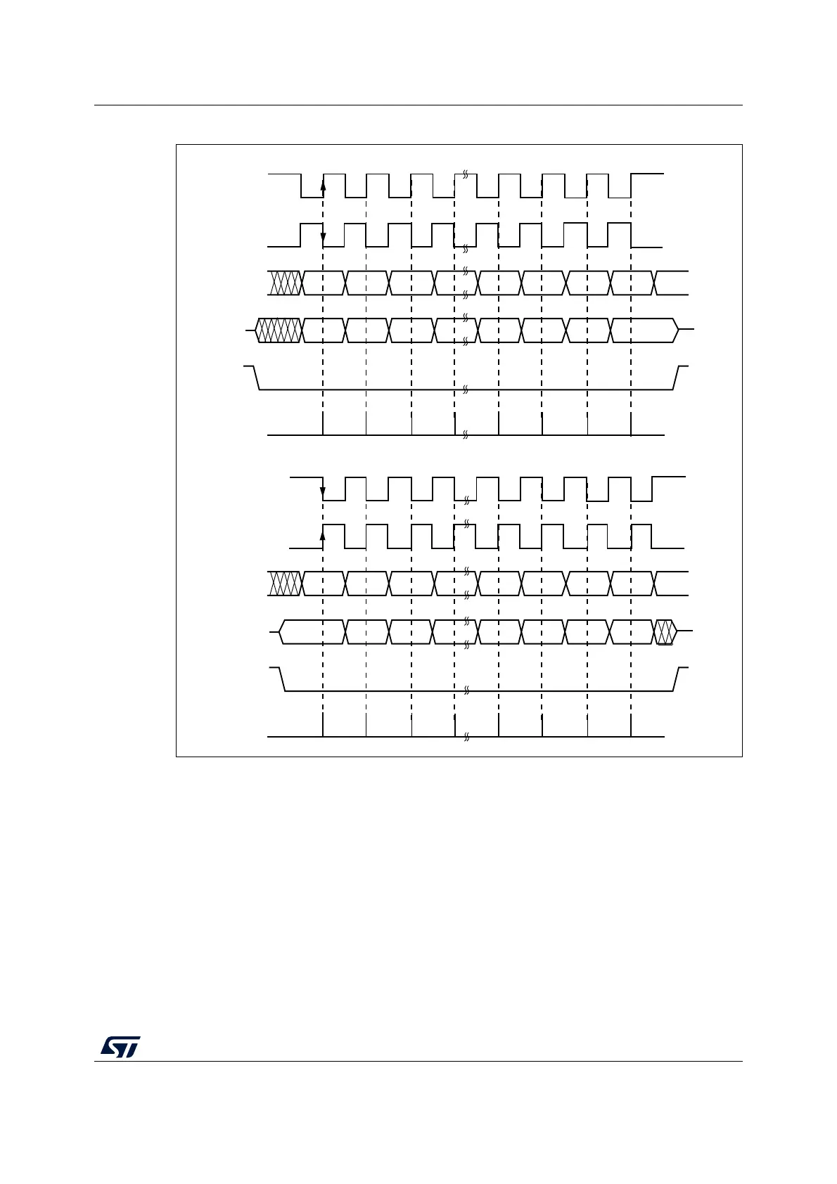
Figure 286. Data clock timing diagram
Note: The order of data bits depends on LSBFIRST bit setting.
Data frame format
The SPI shift register can be set up to shift out MSB-first or LSB-first, depending on the
value of the LSBFIRST bit. Each data frame is 8 or 16 bit long depending on the size of the
data programmed using the DFF bit in the SPI_CR1 register. The selected data frame
format is applicable both for transmission and reception.
CPOL = 1
CPOL = 0
MSBit
LSBit
MSBit
LSBit
MISO
MOSI
NSS
(to slave)
Capture strobe
CPHA =1
CPOL = 1
CPOL = 0
MSBit
LSBit
MSBit
LSBit
MISO
MOSI
NSS
(to slave)
Capture strobe
CPHA =0
ai17154d