Universal synchronous/asynchronous receiver transmitter (USART/UART) RM0367
792/1043 RM0367 Rev 7
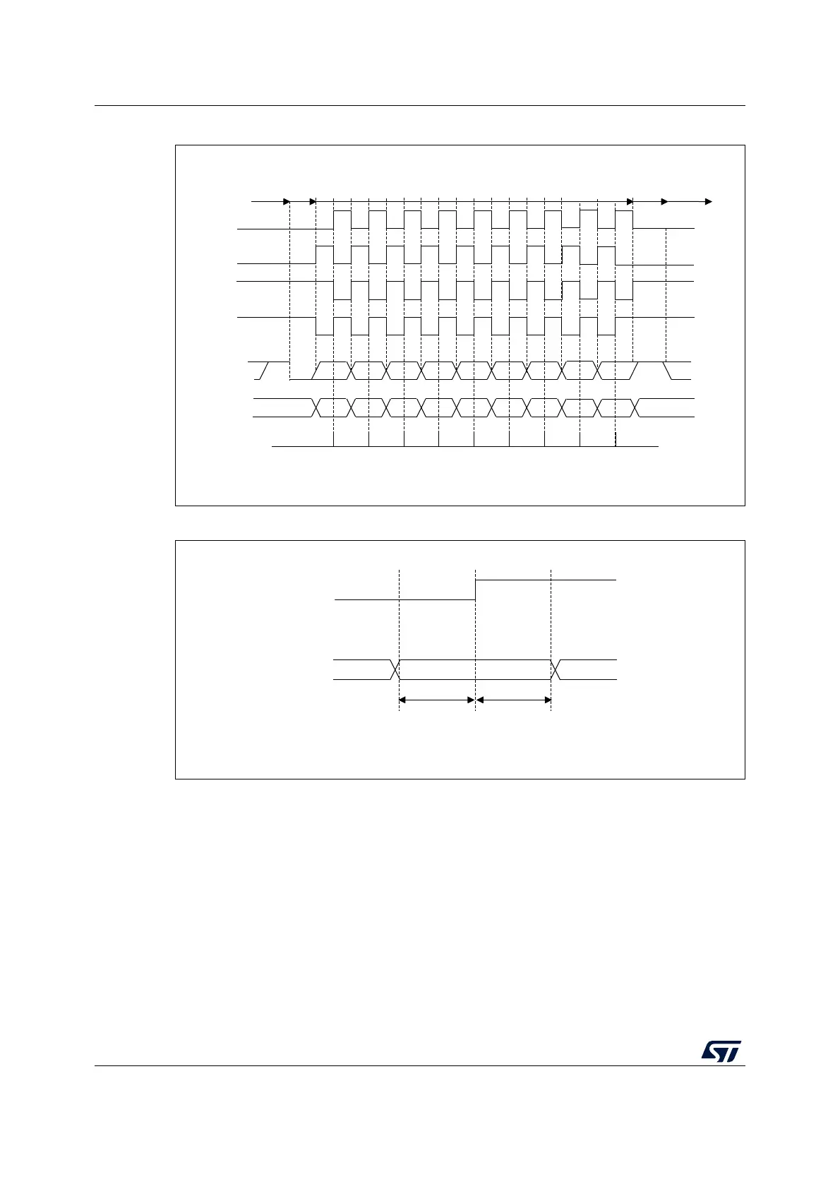
Figure 255. USART data clock timing diagram (M bits = 01)
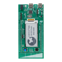
Figure 256. RX data setup/hold time
Note: The function of CK is different in Smartcard mode. Refer to Section 29.5.13: USART
Smartcard mode for more details.
MSv34710V1
0 1 2 3 4 5 6 8
0 1 2 3 4 5 6 8
*
*
*
*
MSB
MSB
LSB
LSBStart
Start Stop
Idle or
preceding
transmission
Idle or next
transmission
*
*LBCL bit controls last data pulse
Capture
strobe
Data on RX
(from slave)
Data on TX
(from master)
Clock (CPOL=1,
CPHA=1)
Clock (CPOL=1,
CPHA=0)
Clock (CPOL=0,
CPHA=1)
Clock (CPOL=0,
CPHA=0)
Stop
M bits =01 (9 data bits)
7
7
MSv31161V2
Data on RX (from slave)
CK
(capture strobe on CK rising
edge in this example)
Valid DATA bit
t
SETUP
t
HOLD
t
SETUP=
t
HOLD
1/16 bit time