Liquid crystal display controller (LCD) RM0367
386/1043 RM0367 Rev 7
17.3 LCD implementation
17.4 LCD functional description
17.4.1 General description
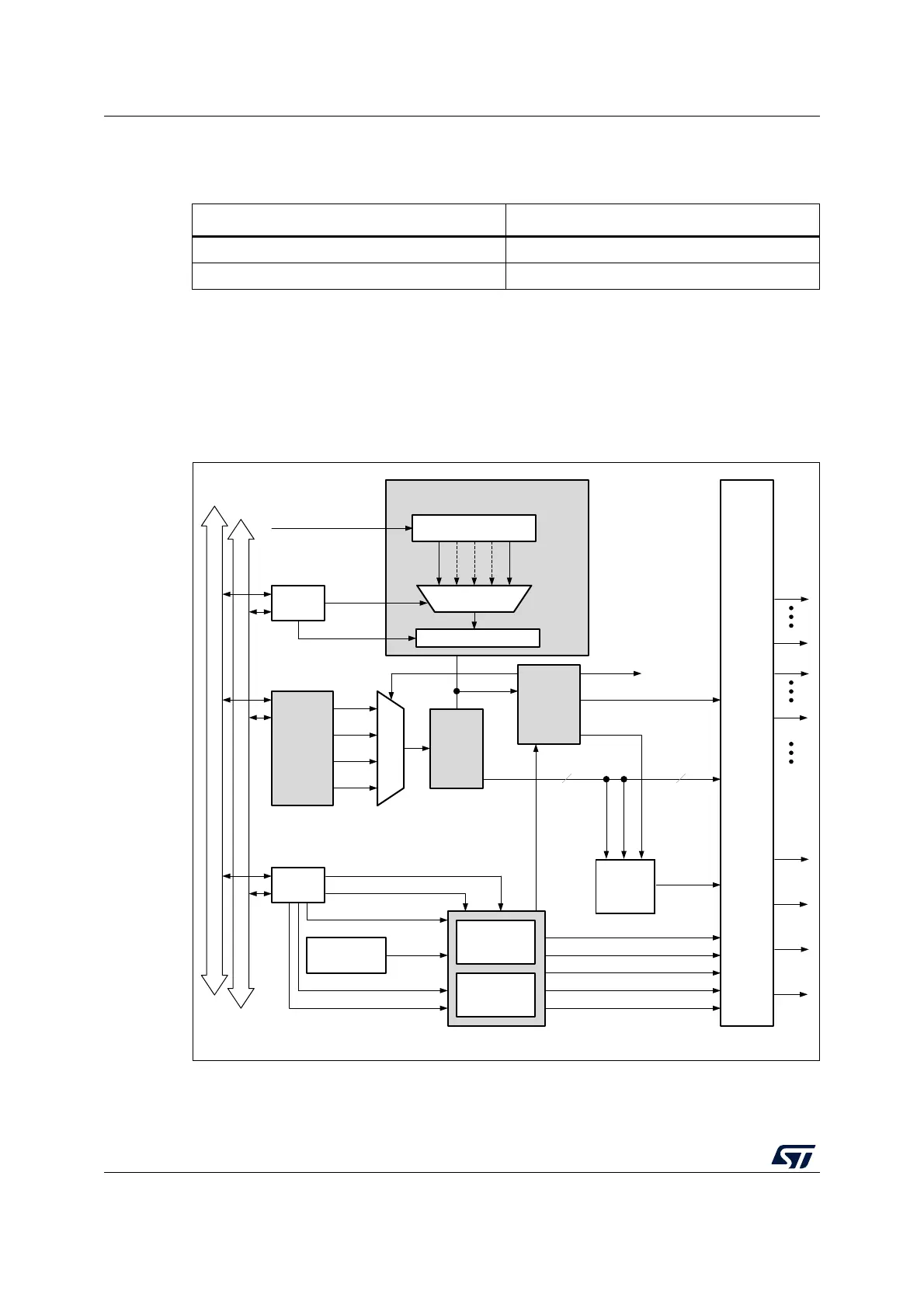
The LCD controller has five main blocks (see Figure 67):
Figure 67. LCD controller block diagram
Note: LCDCLK is the same as RTCCLK. Refer to the RTC/LCD clock description in the RCC
section of this manual.
Table 73. Implementation
Products Segments terminals
Category 5 devices 52 segments
Category 3 devices 32 segments
ADDRESS BUS
DATA BUS
FREQUENCY GENERATOR
MSv33071V2
LCDCLK
COM0
COM3
V
LCD
V
SS
COM[3:0]
PS[3:0]
DIV[3:0]
LCDCLK/32768LCDCLK
ck_div
EN
HD
Analog
switch
array
CC[2:0]
1/3-1/4 V
LCD
2/3 -3/4V
LCD
1/2 V
LCD
BIAS[1:0]
Interrupt
ck_ps
I/O Ports
Analog step-up
converter
READY
VSEL
STATIC
SEG[51:48]
SEG[47:0]
48
SEG [31:28]
COM[7:4]
SEG
MUX
COM
Analog
switch
arrray
VOLTAGE
GENERATOR
CONTRAST
CONTROLLER
LCD
REGS
PULSE GEN
LCD RAM
(32x16 bits)
8-to-1 MUX
SEG
DRIVER
COM
DRIVER
SEG[51:0]
52
SEG [51:48]
CLOCK MUX
16-bit prescaler
Divide by 16 to 31
LCD
REGS
SEG48/
COM4
SEG49/
COM5
SEG50/
COM6
SEG51/
COM7
SEG0
SEG47
 Loading...


