Liquid crystal display controller (LCD) RM0367
392/1043 RM0367 Rev 7
The SEG[n] pin is driven to V
LCD
in phase 0 of the even frame. If pixel n is inactive then the
SEG[n] pin is driven to 2/3 (2/4) V
LCD
in the odd frame or 1/3 (2/4) V
LCD
in the even frame
(current inversion in V
LCD
pad) (see Figure 68).
In case of 1/2 bias, if the pixel is inactive the SEG[n] pin is driven to V
LCD
in the odd and to
V
SS
in the even frame.
When the LCD controller is disabled (LCDEN bit cleared in the LCD_CR register) then the
SEG lines are pulled down to V
SS
.
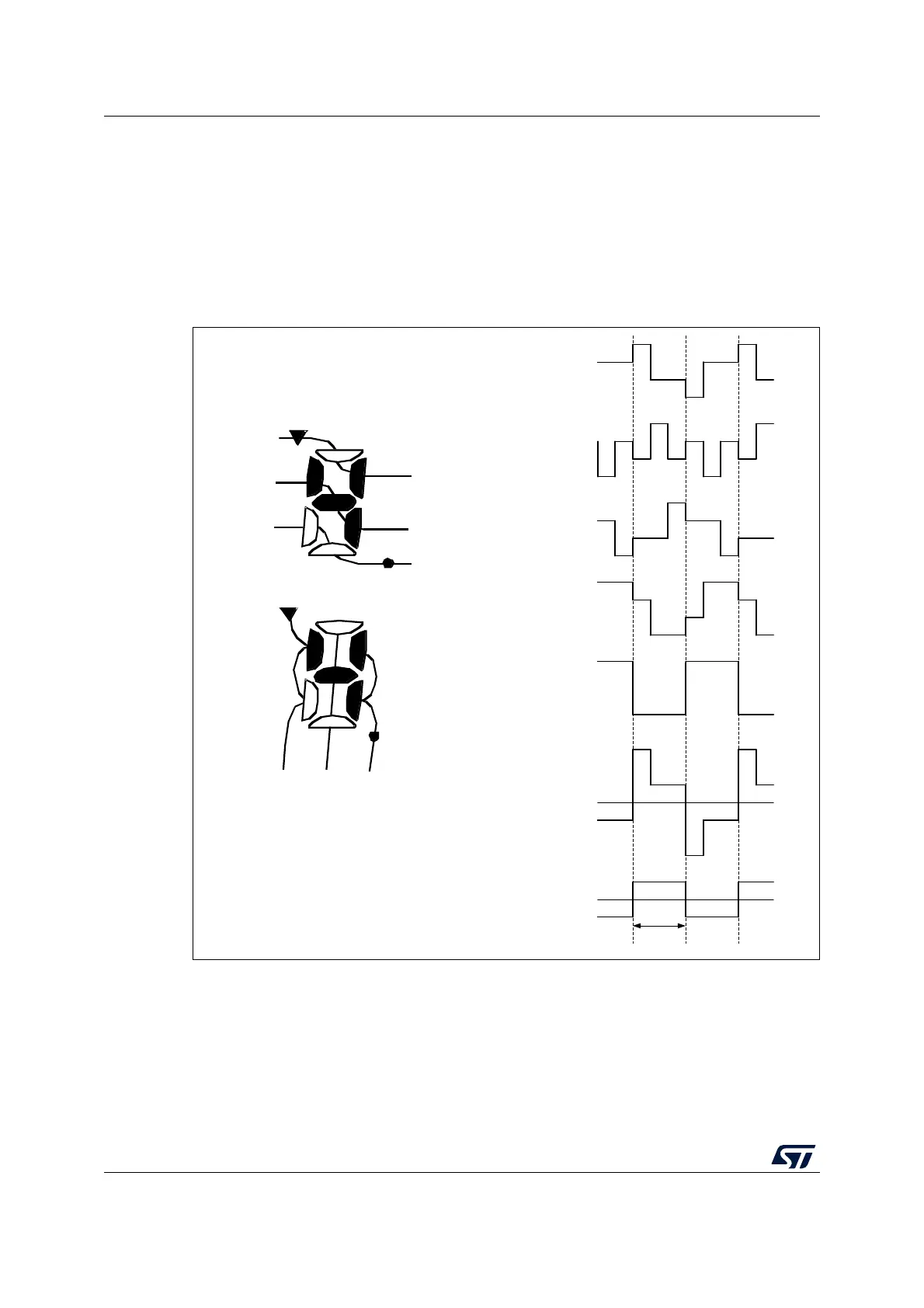
Figure 72. 1/3 duty, 1/3 bias
MS33442V1
3/3 V
2/3 V
1/3 V
0/3 V
PIN
COM0
Liquid crystal display
and terminal connection
COM0
SEG0
SEG2
COM2
COM0-SEG1
selected waveform
3/3 V
2/3 V
1/3 V
0/3 V
-1/3 V
-2/3 V
-3/3 V
COM1
SEG1
3/3 V
2/3 V
1/3 V
0/3 V
PIN
COM1
3/3 V
2/3 V
1/3 V
0/3 V
PIN
COM2
3/3 V
2/3 V
1/3 V
0/3 V
PIN
SEG0
3/3 V
2/3 V
1/3 V
0/3 V
PIN
SEG1
COM0-SEG0
non selected waveform
1/3 V
0/3 V
-1/3 V
1 frame
 Loading...


