Liquid crystal display controller (LCD) RM0367
388/1043 RM0367 Rev 7
The frame frequency must be selected to be within a range of around ~30 Hz to ~100 Hz
and is a compromise between power consumption and the acceptable refresh rate. In
addition, a dedicated blink prescaler selects the blink frequency. This frequency is defined
as:
f
BLINK
= f
ck_div
/2
(BLINKF + 3)
,
with BLINKF[2:0] = 0, 1, 2, ... ,7
The blink frequency achieved is in the range of 0.5 Hz, 1 Hz, 2 Hz or 4 Hz.
17.4.3 Common driver
Common signals are generated by the common driver block (see Figure 67).
COM signal bias
Each COM signal has identical waveforms, but different phases. It has its max amplitude
V
LCD
or V
SS
only in the corresponding phase of a frame cycle, while during the other
phases, the signal amplitude is:
• 1/4 V
LCD
or 3/4 V
LCD
in case of 1/4 bias
• 1/3 V
LCD
or 2/3 V
LCD
in case of 1/3 bias
• and 1/2 V
LCD
in case of 1/2 bias.
Selection between 1/2, 1/3 and 1/4 bias mode can be done through the BIAS bits in the
LCD_CR register.
A pixel is activated when both of its corresponding common and segment lines are active
during the same phase, it means when the voltage difference between common and
segment is maximum during this phase. Common signals are phase inverted in order to
reduce EMI. As shown in Figure 68, with phase inversion, there is a mean voltage of 1/2
V
LCD
at the end of every odd cycle.
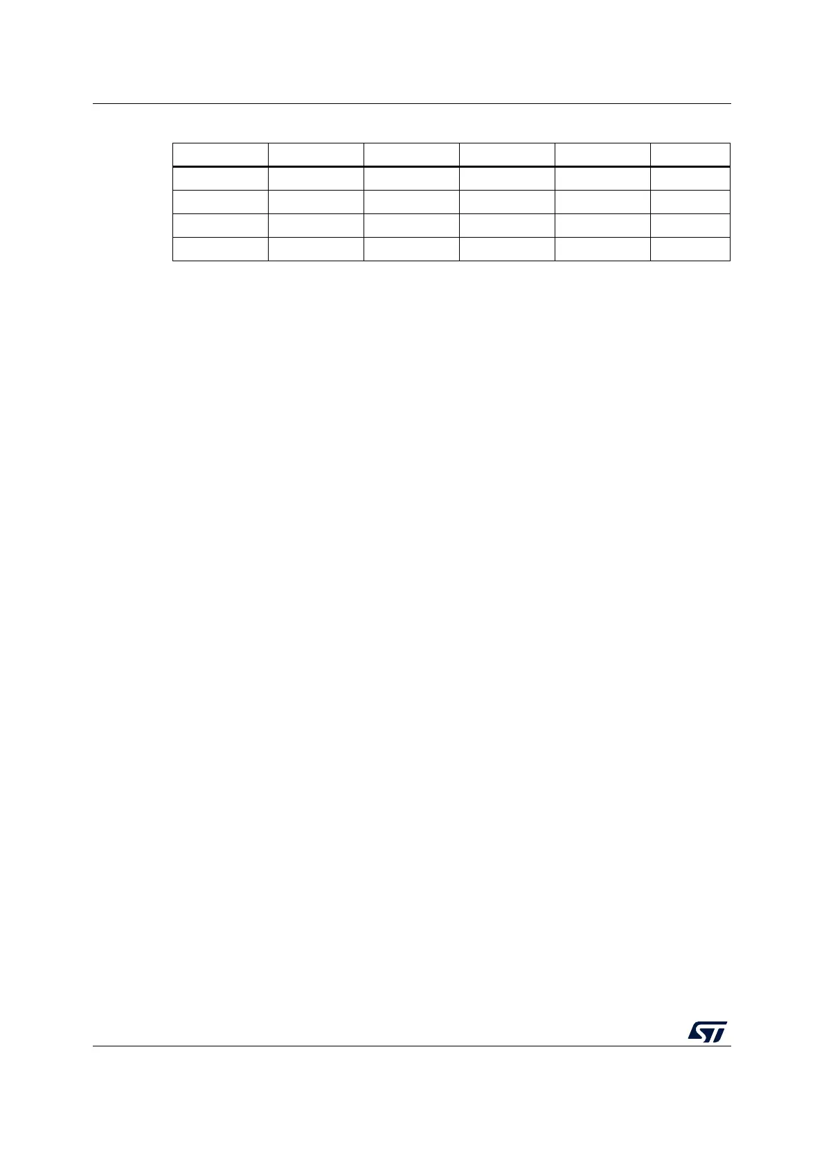
1.00 MHz 7 3 2432 1/4 102.80 Hz
1.00 MHz 7 10 3328 1/3 100.16 Hz
1.00 MHz 8 3 4864 1/2 102.80 Hz
1.00 MHz 9 3 9728 static 102.80 Hz
Table 74. Example of frame rate calculation (continued)
LCDCLK PS[3:0] DIV[3:0] Ratio Duty f
frame