Direct memory access controller (DMA) RM0367
284/1043 RM0367 Rev 7
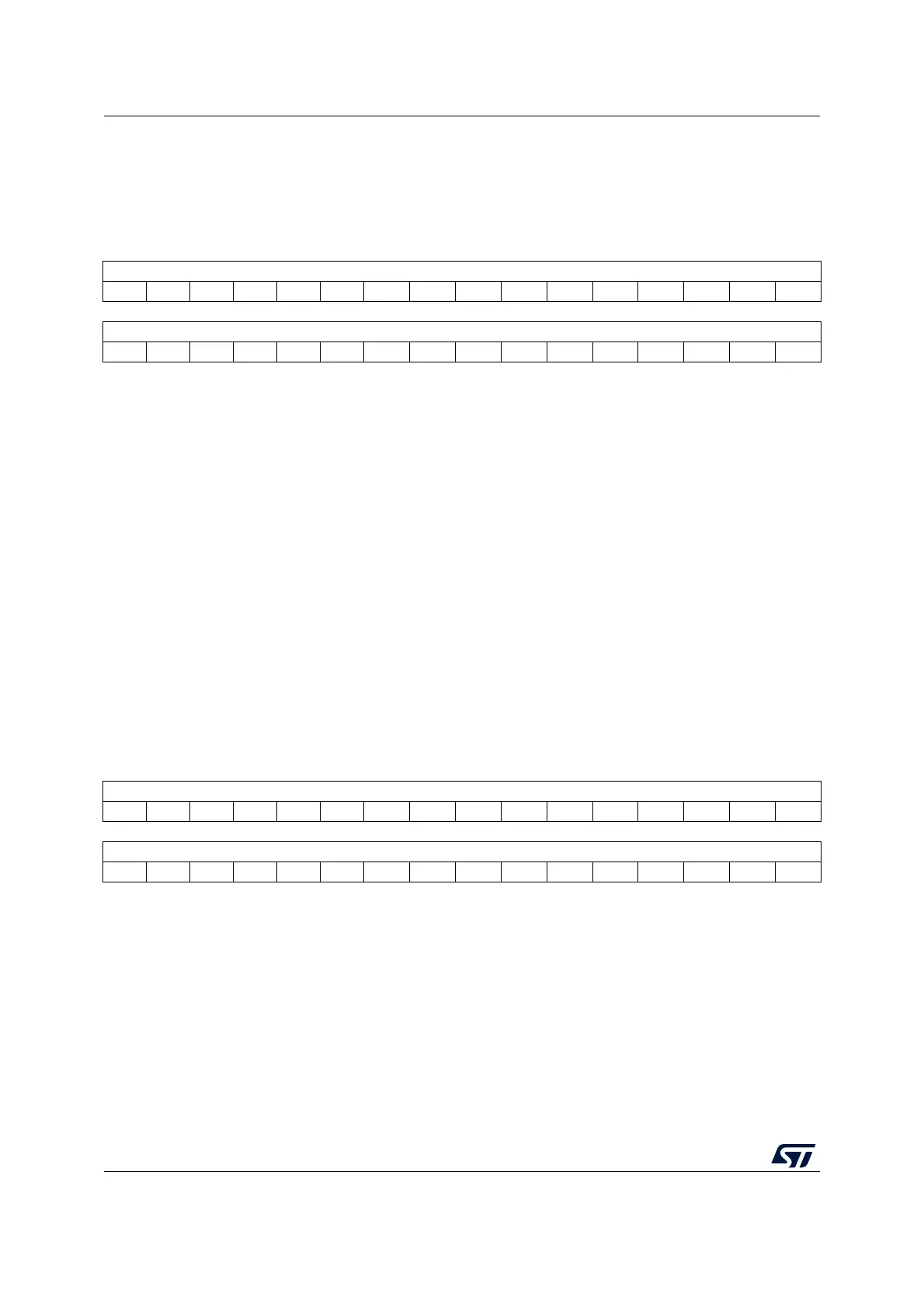
11.6.5 DMA channel x peripheral address register (DMA_CPARx)
Address offset: 0x10 + 0x14 * (x - 1), (x = 1 to 7)
Reset value: 0x0000 0000
11.6.6 DMA channel x memory address register (DMA_CMARx)
Address offset: 0x14 + 0x14 * (x - 1), (x = 1 to 7)
Reset value: 0x0000 0000
31 30 29 28 27 26 25 24 23 22 21 20 19 18 17 16
PA[31:16]
rw rw rw rw rw rw rw rw rw rw rw rw rw rw rw rw
1514131211109876543210
PA[15:0]
rw rw rw rw rw rw rw rw rw rw rw rw rw rw rw rw
Bits 31:0 PA[31:0]: peripheral address
It contains the base address of the peripheral data register from/to which the data will be
read/written.
When PSIZE[1:0] = 01 (16 bits), bit 0 of PA[31:0] is ignored. Access is automatically aligned
to a half-word address.
When PSIZE = 10 (32 bits), bits 1 and 0 of PA[31:0] are ignored. Access is automatically
aligned to a word address.
In memory-to-memory mode, this register identifies the memory destination address if
DIR = 1 and the memory source address if DIR = 0.
In peripheral-to-peripheral mode, this register identifies the peripheral destination address
DIR = 1 and the peripheral source address if DIR = 0.
Note: this register is set and cleared by software.
It must not be written when the channel is enabled (EN = 1).
It is not read-only when the channel is enabled (EN = 1).
31 30 29 28 27 26 25 24 23 22 21 20 19 18 17 16
MA[31:16]
rw rw rw rw rw rw rw rw rw rw rw rw rw rw rw rw
1514131211109876543210
MA[15:0]
rw rw rw rw rw rw rw rw rw rw rw rw rw rw rw rw