RM0367 Rev 7 227/1043
RM0367 Clock recovery system (CRS)
236
8.4 CRS functional description
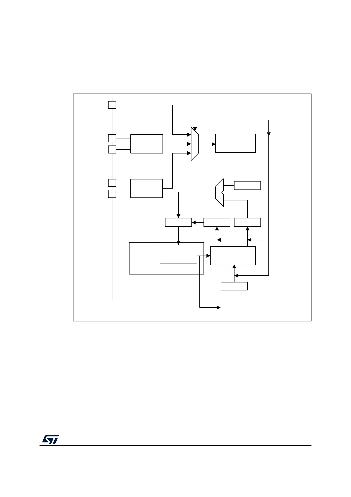
8.4.1 CRS block diagram
Figure 19. CRS block diagram
8.4.2 Synchronization input
The CRS synchronization (SYNC) source, selectable through the CRS_CFGR register, can
be the signal from the LSE clock or the USB SOF signal. For a better robustness of the
SYNC input, a simple digital filter (2 out of 3 majority votes, sampled by the RC48 clock) is
implemented to filter out any glitches. This source signal also has a configurable polarity
and can then be divided by a programmable binary prescaler to obtain a synchronization
signal in a suitable frequency range (usually around 1 kHz).
For more information on the CRS synchronization source configuration, refer to
Section 8.7.2: CRS configuration register (CRS_CFGR).
It is also possible to generate a synchronization event by software, by setting the SWSYNC
bit in the CRS_CR register.
MSv34708V1
LSE
USB
SYNCSRC
GPIO
OSC32_IN
OSC32_OUT
USB_DP
USB_DM
SYNC divider
(/1,/2,/4,…,/128)
SWSYNC
RELOAD
SYNC
16-bit counter
FECAP
RC 48 MHz
HSI48
RCC
CRS_SYNC
FELIM
TRIM FEDIR
To USB
To RNG