Analog-to-digital converter (ADC) RM0367
334/1043 RM0367 Rev 7
Main features
• Supported temperature range: –40 to 125 °C
• Linearity: ±2 °C max., precision depending on calibration
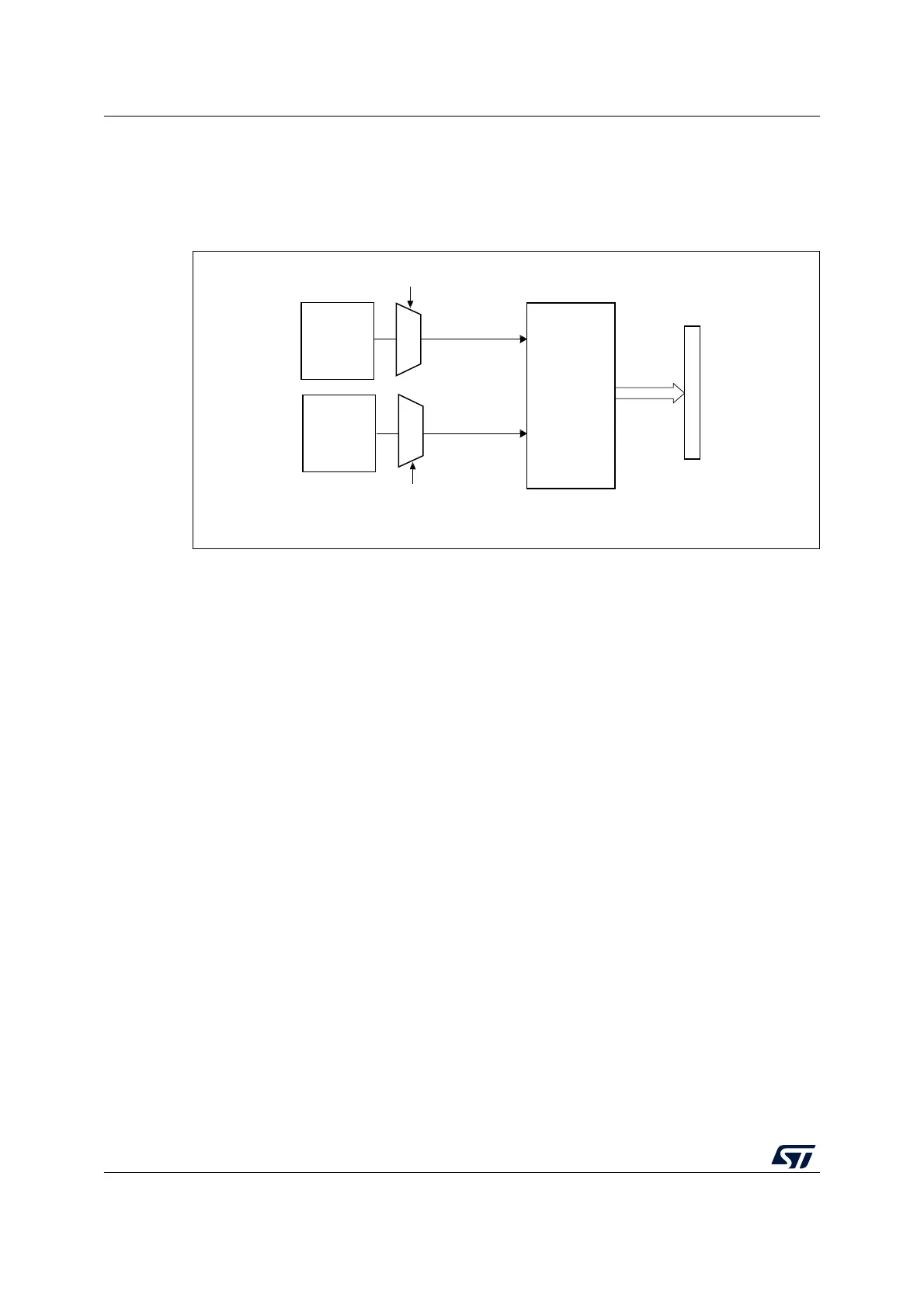
Figure 57. Temperature sensor and V
REFINT
channel block diagram
Reading the temperature
1. Select the ADC V
IN
[18] input channel.
2. Select an appropriate sampling time specified in the device datasheet (T
S_temp
).
3. Set the TSEN bit in the ADC_CCR register to wake up the temperature sensor from
power down mode and wait for its stabilization time (t
START
).
For code example, refer to A.8.16: Temperature configuration code example.
4. Start the ADC conversion by setting the ADSTART bit in the ADC_CR register (or by
external trigger).
5. Read the resulting V
SENSE
data in the ADC_DR register.
6. Calculate the temperature using the following formula
Where:
• TS_CAL2 is the temperature sensor calibration value acquired at TS_CAL2_TEMP
(refer to the datasheet for TS_CAL2 value)
• TS_CAL1 is the temperature sensor calibration value acquired at TS_CAL1_TEMP
(refer to the datasheet for TS_CAL1 value)
• TS_DATA is the actual temperature sensor output value converted by ADC
Refer to the specific device datasheet for more information about TS_CAL1 and
TS_CAL2 calibration points.
For code example, refer to A.8.17: Temperature computation code example.
MS34765V2
V
SENSE
TSEN control bit
Address/data bus
converted
data
V
REFINT
ADC V
IN
[18]
Temperature
sensor
Internal
power block
ADC
VREFEN control bit
ADC V
IN
[17]
Temperature in °C()
TS_CAL2_TEMP TS_CAL1_TEMP–
TS_CAL2 TS_CAL1–
----------------------------------------------------------------------------------------------------
TS_DATA TS_CAL1–()TS_CAL1_TEMP+×=