Digital-to-analog converter (DAC) RM0367
354/1043 RM0367 Rev 7
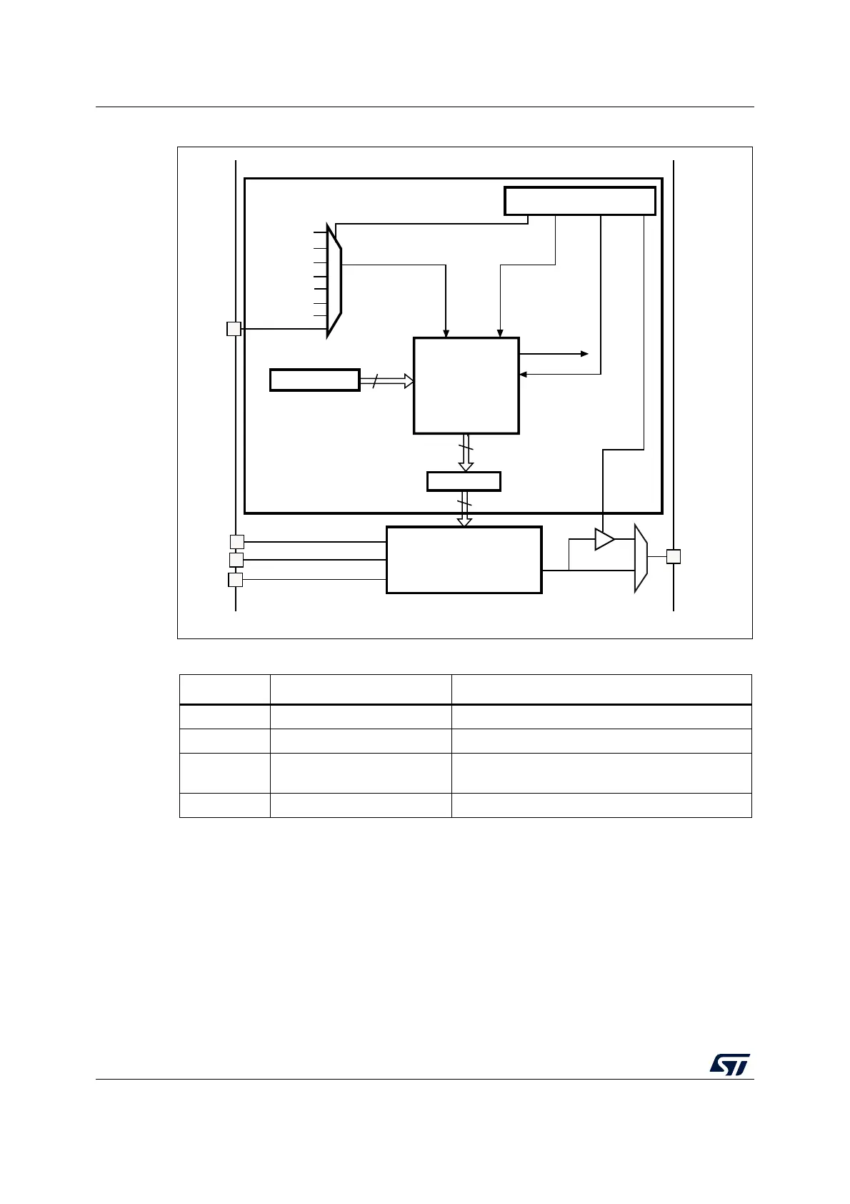
Figure 58. DAC block diagram
Note: Once DAC_Channelx is enabled, the corresponding GPIO pin (PA4 or PA5) is automatically
connected to the analog converter output (DAC_OUTx). In order to avoid parasitic
consumption, PA4/PA5 pin should first be configured to analog (AIN).
Table 69. DAC pins
Name Signal type Remarks
V
DDA
Input, analog supply Analog power supply
V
SSA
Input, analog supply ground Ground for analog power supply
V
REF+
Input, analog positive
reference
The higher/positive reference voltage for the DAC1
DAC_OUT1/2 Analog output signal DAC channelx analog output
MS33718V3
V
DDA
V
REF+
DAC_ OU T1/2
Control logic
DHRx
12-bit
12-bit
DM A req ue stx
TSELx[2:0] bits
EXTI_9
DMAENx
TENx
DORx
Digital-to-analog
converterx
12-bit
DAC control register
Trigger selector
BOFF
TIM6_TRGO
TIM21_TRGO
TIM2_TRGO
SWTRIGx
V
SSA
TIM3_TRGO
TIM7_TRGO
TIM3_CH3
 Loading...


