RM0367 Rev 7 501/1043
RM0367 General-purpose timers (TIM2/TIM3)
546
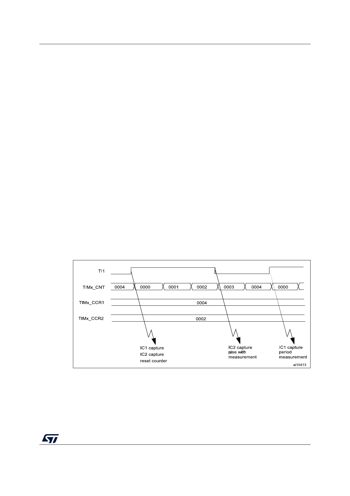
21.3.6 PWM input mode
This mode is a particular case of input capture mode. The procedure is the same except:
• Two ICx signals are mapped on the same TIx input.
• These 2 ICx signals are active on edges with opposite polarity.
• One of the two TIxFP signals is selected as trigger input and the slave mode controller
is configured in reset mode.
For example, one can measure the period (in TIMx_CCR1 register) and the duty cycle (in
TIMx_CCR2 register) of the PWM applied on TI1 using the following procedure (depending
on CK_INT frequency and prescaler value):
1. Select the active input for TIMx_CCR1: write the CC1S bits to 01 in the TIMx_CCMR1
register (TI1 selected).
2. Select the active polarity for TI1FP1 (used both for capture in TIMx_CCR1 and counter
clear): write the CC1P to ‘0’ and the CC1NP bit to ‘0’ (active on rising edge).
3. Select the active input for TIMx_CCR2: write the CC2S bits to 10 in the TIMx_CCMR1
register (TI1 selected).
4. Select the active polarity for TI1FP2 (used for capture in TIMx_CCR2): write the CC2P
bit to ‘1’ and the CC2NP bit to ’0’(active on falling edge).
5. Select the valid trigger input: write the TS bits to 101 in the TIMx_SMCR register
(TI1FP1 selected).
6. Configure the slave mode controller in reset mode: write the SMS bits to 100 in the
TIMx_SMCR register.
7. Enable the captures: write the CC1E and CC2E bits to ‘1 in the TIMx_CCER register.
For code example, refer to A.11.5: PWM input configuration code example.
Figure 134. PWM input mode timing