RM0367 Rev 7 697/1043
RM0367 Inter-integrated circuit (I2C) interface
763
If SMBus feature is supported: the additional optional SMBus Alert pin (SMBA) is also
available.
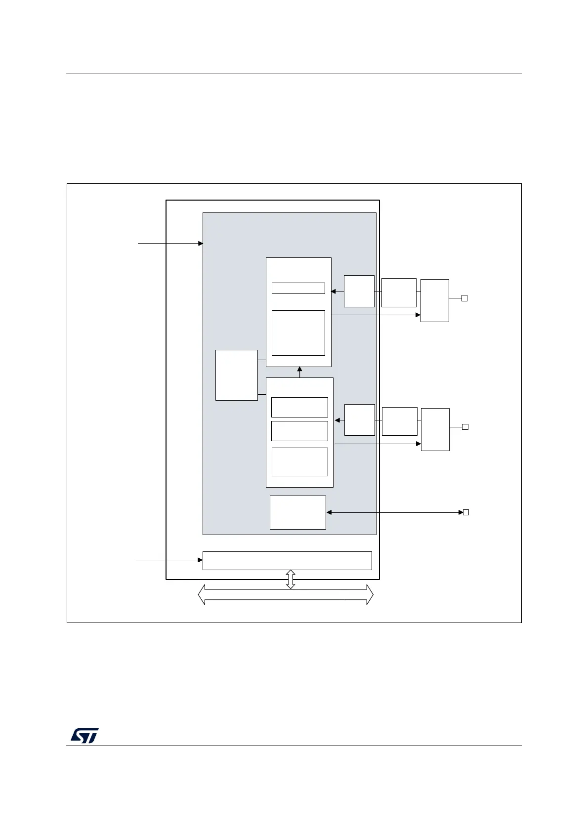
28.4.1 I2C1/3 block diagram
The block diagram of the I2C1 interface is shown in Figure 211.
Figure 211. I2C1/3 block diagram
The I2C1/3 is clocked by an independent clock source which allows the I2C to operate
independently from the PCLK frequency.
For I2C I/Os supporting 20mA output current drive for Fast-mode Plus operation, the driving
capability is enabled through control bits in the system configuration controller (SYSCFG).
Refer to Section 28.3: I2C implementation.
MSv46198V2
I2CCLK
Wakeup
on
address
match
SMBUS
PEC
generation/
check
Shift register
Data control
SMBus
Timeout
check
Clock control
Master clock
generation
Slave clock
stretching
SMBus Alert
control/status
Digital
noise
filter
I2C_SCL
I2C_SMBA
Registers
APB bus
GPIO
logic
Analog
noise
filter
Digital
noise
filter
I2C_SDA
GPIO
logic
Analog
noise
filter
i2c_pclk
i2c_ker_ck
PCLK