General-purpose timers (TIM21/22) RM0367
576/1043 RM0367 Rev 7
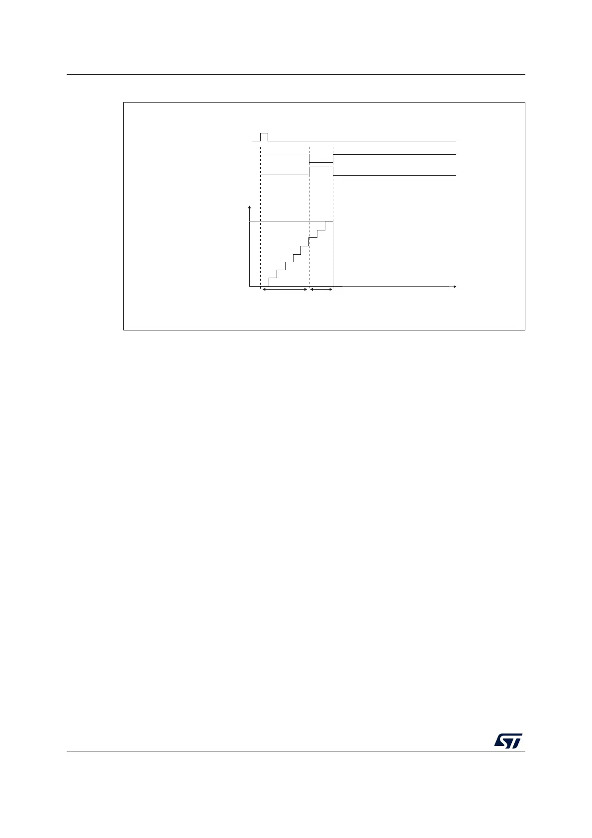
Figure 184. Example of one pulse mode
For example one may want to generate a positive pulse on OC1 with a length of t
PULSE
and
after a delay of t
DELAY
as soon as a positive edge is detected on the TI2 input pin.
Use TI2FP2 as trigger 1:
1. Map TI2FP2 to TI2 by writing CC2S=’01’ in the TIMx_CCMR1 register.
2. TI2FP2 must detect a rising edge, write CC2P=’0’ and CC2NP = ‘0’ in the TIMx_CCER
register.
3. Configure TI2FP2 as trigger for the slave mode controller (TRGI) by writing TS=’110’ in
the TIMx_SMCR register.
4. TI2FP2 is used to start the counter by writing SMS to ‘110’ in the TIMx_SMCR register
(trigger mode).
The OPM waveform is defined by writing the compare registers (taking into account the
clock frequency and the counter prescaler).
• The t
DELAY
is defined by the value written in the TIMx_CCR1 register.
• The t
PULSE
is defined by the difference between the auto-reload value and the compare
value (TIMx_ARR - TIMx_CCR1+1).
• Let’s say one want to build a waveform with a transition from ‘0’ to ‘1’ when a compare
match occurs and a transition from ‘1’ to ‘0’ when the counter reaches the auto-reload
value. To do this PWM mode 2 must be enabled by writing OC1M=’111’ in the
TIMx_CCMR1 register. Optionally the preload registers can be enabled by writing
OC1PE=’1’ in the TIMx_CCMR1 register and ARPE in the TIMx_CR1 register. In this
case one has to write the compare value in the TIMx_CCR1 register, the auto-reload
value in the TIMx_ARR register, generate an update by setting the UG bit and wait for
external trigger event on TI2. CC1P is written to ‘0’ in this example.
In our example, the DIR and CMS bits in the TIMx_CR1 register should be low.
For code example, refer to A.11.16: One-Pulse mode code example.
MS31099V1
TI2
OC1REF
Counter
t
0
TIM1_ARR
TIM1_CCR1
OC1
t
DELAY
t
PULSE
 Loading...


