RM0367 Rev 7 461/1043
RM0367 AES hardware accelerator (AES)
466
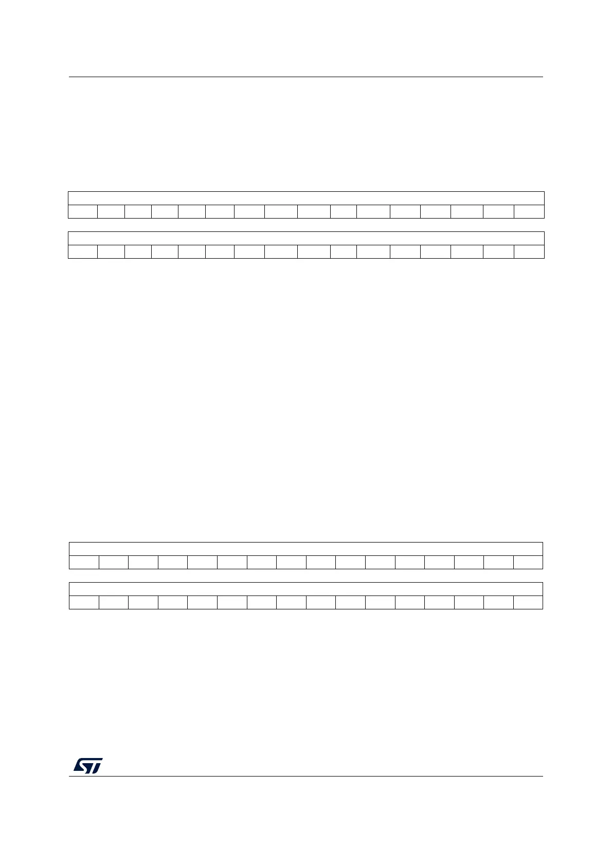
19.7.3 AES data input register (AES_DINR)
Address offset: 0x08
Reset value: 0x0000 0000
Only 32-bit access type is supported.
19.7.4 AES data output register (AES_DOUTR)
Address offset: 0x0C
Reset value: 0x0000 0000
Only 32-bit access type is supported.
31 30 29 28 27 26 25 24 23 22 21 20 19 18 17 16
DIN[x+31:x+16]
rw rw rw rw rw rw rw rw rw rw rw rw rw rw rw rw
15 14 13 12 11 10 9 8 7 6 5 4 3 2 1 0
DIN[x+15:x]
rw rw rw rw rw rw rw rw rw rw rw rw rw rw rw rw
Bits 31:0
DIN[x+31:x]: One of fo ur 32-bit w ords of a 128-bit i nput data block be ing written into the peripheral
This bitfield feeds a 32-bit input buffer. A 4-fold sequential write to this bitfield during the input phase
virtually writes a complete 128-bit block of input data to the AES peripheral. Upon each write, the
data from the input buffer are handled by the data swap block according to the DATATYPE[1:0]
bitfield, then written into the AES core 128-bit input buffer.
The substitution for “x”, from the first to the fourth write operation, is: 96, 64, 32, and 0. In other
words, data from the first to the fourth write operation are: DIN[127:96], DIN[95:64], DIN[63:32], and
DIN[31:0].
The data signification of the input data block depends on the AES operating mode:
- Mode 1 (encryption): plaintext
- Mode 2 (key derivation): the bitfield is not used (AES_KEYRx registers used for input)
- Mode 3 (decryption) and Mode 4 (key derivation then single decryption): ciphertext
The data swap operation is described in Section 19.4.10: AES data registers and data swapping on
page 451.
31 30 29 28 27 26 25 24 23 22 21 20 19 18 17 16
DOUT[x+31:x+16]
rrrrrrrrrrrrrrrr
1514131211109876543210
DOUT[x+15:0]
rrrrrrrrrrrrrrrr