RM0367 Rev 7 391/1043
RM0367 Liquid crystal display controller (LCD)
413
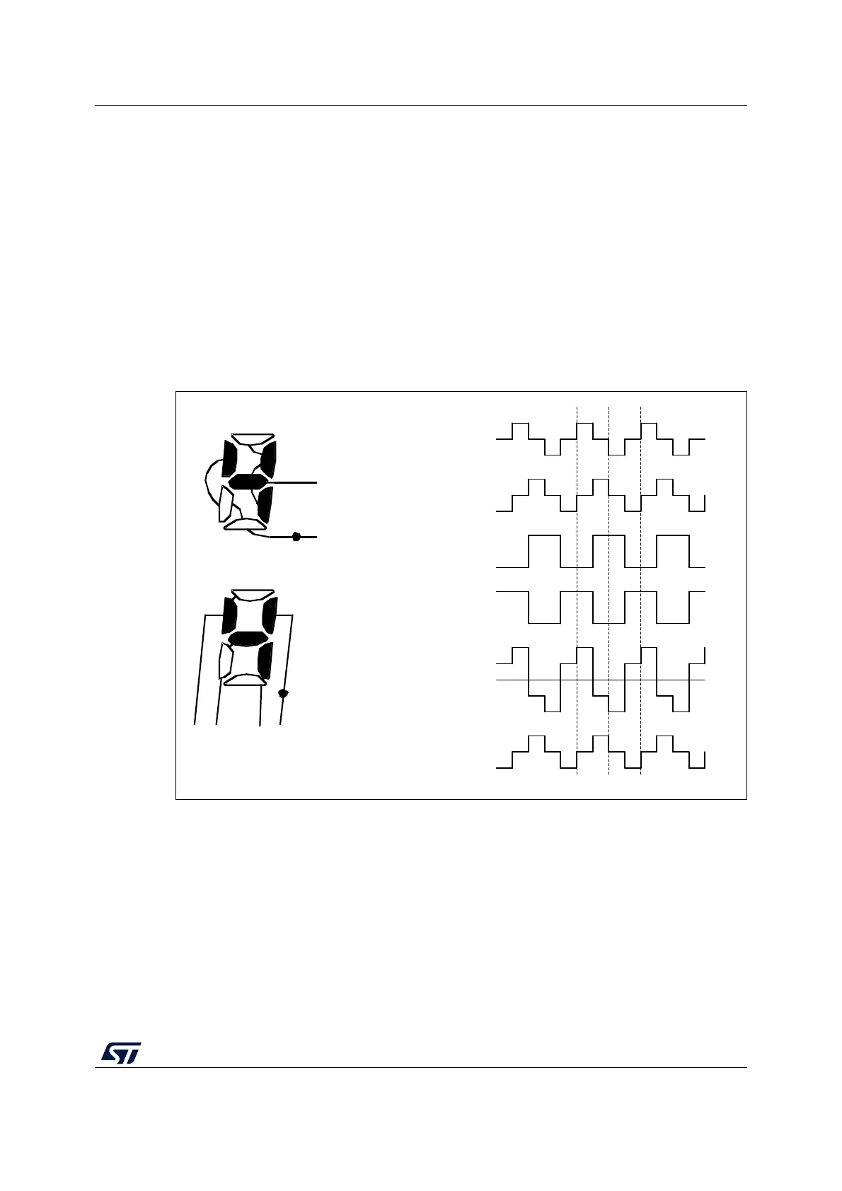
In this mode, the segment terminals are multiplexed and each of them control four pixels. A
pixel is activated only when both of its corresponding SEG and COM lines are active in the
same phase. In case of 1/4 duty, to deactivate pixel 0 connected to COM[0] the SEG[0]
needs to be inactive during the phase 0 when COM[0] is active. To activate pixel 0
connected to COM[1], the SEG[0] needs to be active during phase 1 when COM[1] is active
(see Figure 73). To activate pixels from 0 to 51 connected to COM[0], SEG[0:51] need to be
active during phase 0 when COM[0] is active. These considerations can be extended to the
other pixels.
8 to 1 Mux
When COM[0] is active the common driver block, also drives the 8 to 1 mux shown in
Figure 67 in order to select the content of first two RAM register locations. When COM[7] is
active, the output of the 8 to 1 mux is the content of the last two RAM locations.
Figure 71. 1/2 duty, 1/2 bias
17.4.4 Segment driver
The segment driver block controls the SEG lines according to the pixel data coming from the
8 to 1 mux driven in each phase by the common driver block.
In the case of 1/4 or 1/8 duty
When COM[0] is active, the pixel information (active/inactive) related to the pixel connected
to COM[0] (content of the first two LCD_RAM locations) goes through the 8 to 1 mux.
The SEG[n] pin n [0 to 51] is driven to V
SS
(indicating pixel n is active when COM[0] is
active) in phase 0 of the odd frame.
MS33441V1
2/2 V
1/2 V
0/2 V
PIN
COM0
Liquid crystal display
and terminal connection
COM0
SEG0
SEG1
SEG2
SEG3
COM0-SEG1
non selected waveform
COM1
PIN
COM1
2/2 V
1/2 V
0/2 V
PIN
SEG0
2/2 V
0/2 V
PIN
SEG1
2/2 V
0/2V
COM0-SEG0
selected waveform
2/2 V
1/2 V
0/2 V
-1/2 V
-2/2 V
1/2 V
0/2 V
-1/2 V