Comparator (COMP) RM0367
378/1043 RM0367 Rev 7
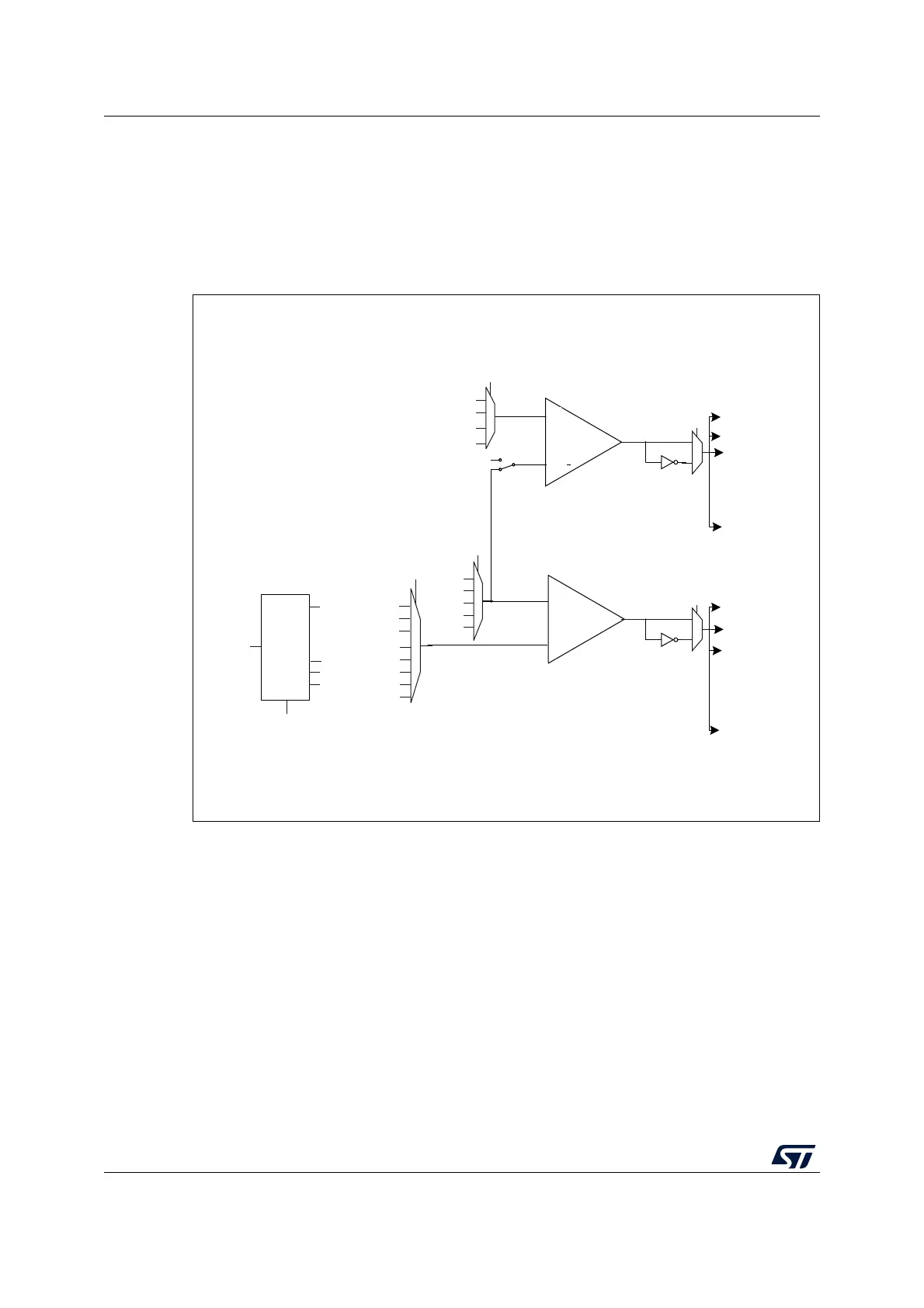
16.3 COMP functional description
16.3.1 COMP block diagram
The block diagram of the comparators is shown in Figure 66: Comparator 1 and 2 block
diagrams.
Figure 66. Comparator 1 and 2 block diagrams
16.3.2 COMP pins and internal signals
The I/Os used as comparators inputs must be configured in analog mode in the GPIOs
registers.
The comparator output can be connected to the I/Os using the alternate function channel
given in “Alternate function mapping” table in the datasheet.
The output can also be internally redirected to a variety of timer input for the following
purposes:
• Input capture for timing measures
It is possible to have the comparator output simultaneously redirected internally and
externally.
-
+
-
+
COMP1POLARITY
COMP1VALUE
COMP1INNSEL
PA1
COMP1WM
COMP2INPSEL
PA3
PB4
PB6
PB7
VREFINT
¼ VREFINT
½ VREFINT
¾ VREFINT
PA2
PA4 (DAC1)
PA5 (DAC2)
PB3
COMP2INNSEL
COMP2VALUE
TIM2_ETR
TIM2_CH4
TIM21_ETR
TIM21_CH2
TIM22_ETR
TIM22_CH1
LPTIM_ETR
LPTIM_CH2
TIM2_ETR
TIM2_CH4
TIM21_ETR
TIM21_CH2
TIM22_ETR
TIM22_CH1
LPTIM_ETR
LPTIM_CH2
VREFINT
PA0
PA4 (DAC1)
PA5 (DAC2)
Wakeup
EXTI line 21
Wakeup
EXTI line 22
COMP1
COMP2
MSv33715V5
-
+
GPIOx
GPIOx
COMP2POLARITY
PB5
Scaler
VREFINT
ENBUF_
VREFINT
_COMP2