Analog-to-digital converter (ADC) RM0367
310/1043 RM0367 Rev 7
The input clock of the analog ADC can be selected between two different clock sources (see
Figure 35: ADC clock scheme to see how the PCLK clock and the ADC asynchronous clock
are enabled):
a) The ADC clock can be a specific clock source, named “ADC asynchronous clock“
which is independent and asynchronous with the APB clock.
Refer to RCC Section for more information on generating this clock source.
To select this scheme, bits CKMODE[1:0] of the ADC_CFGR2 register must be
reset.
b) The ADC clock can be derived from the APB clock of the ADC bus interface,
divided by a programmable factor (1, 2 or 4) according to bits CKMODE[1:0].
To select this scheme, bits CKMODE[1:0] of the ADC_CFGR2 register must be
different from “00”.
For code example, refer to A.8.4: ADC clock selection code example.
In option a), the generated ADC clock can eventually be divided by a prescaler (1, 2, 4, 6, 8,
10, 12, 16, 32, 64, 128, 256) when programming the bits PRESC[3:0] in the ADC_CCR
register).
Option a) has the advantage of reaching the maximum ADC clock frequency whatever the
APB clock scheme selected.
Option b) has the advantage of bypassing the clock domain resynchronizations. This can be
useful when the ADC is triggered by a timer and if the application requires that the ADC is
precisely triggered without any uncertainty (otherwise, an uncertainty of the trigger instant is
added by the resynchronizations between the two clock domains).
Caution: When selecting CKMODE[1:0] = 11 (PCLK divided by 1), the user must ensure that the
PCLK has a 50% duty cycle. This is done by selecting a system clock with a 50% duty cycle
and configuring the APB prescaler in bypass modes in the RCC (refer to there Reset and
clock controller section). If an internal source clock is selected, the AHB and APB prescalers
do not divide the clock.
Low frequency
When selecting an analog ADC clock frequency lower than 3.5 MHz, it is mandatory to first
enable the Low Frequency Mode by setting bit LFMEN = 1 into the ADC_CCR register
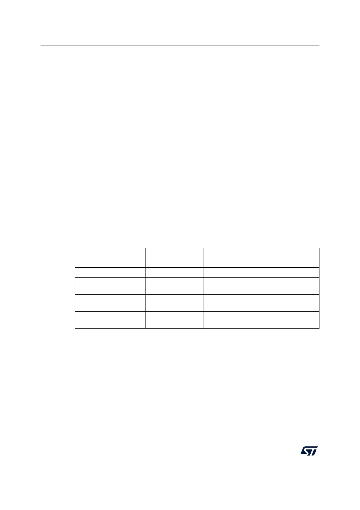
Table 61. Latency between trigger and start of conversion
(1)
1. Refer to the device datasheet for the maximum ADC_CLK frequency.
ADC clock source CKMODE[1:0]
Latency between the trigger event
and the start of conversion
HSI16 MHz clock 00 Latency is not deterministic (jitter)
PCLK divided by 2 01
Latency is deterministic (no jitter) and equal to
4.25 ADC clock cycles
PCLK divided by 4 10
Latency is deterministic (no jitter) and equal to
4.125 ADC clock cycles
PCLK divided by 1 11
Latency is deterministic (no jitter) and equal to
4.5 ADC clock cycles