RM0367 Rev 7 73/1043
RM0367 Flash program memory and data EEPROM (FLASH)
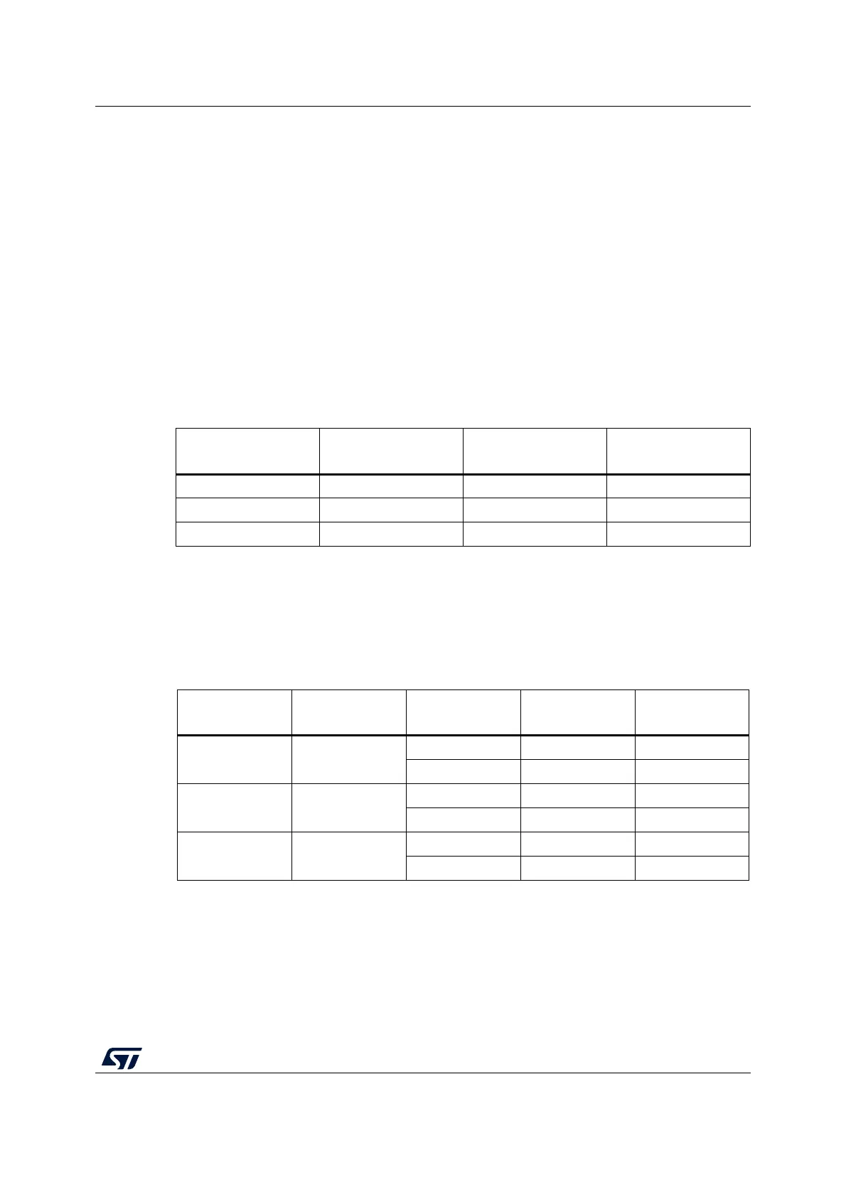
122
You can read the NVM by word (4 bytes), half-word (2 bytes) or byte.
When the NVM features only one bank, it is not possible to read the NVM during a
write/erase operation. If a write/erase operation is ongoing, the reading will be in a wait state
until the write/erase operation completes, stalling the master that requested the read
operation, except when the address is read-protected. In this case, the error is sent to the
master by a hard fault or a memory interface flag; no stall is generated and no read is
waiting.
When two banks are available (category 5 devices), read operations from one bank can be
performed while write or erase operations are performed on the other bank.
Relation between CPU frequency/Operation mode/NVM read time
The device (and the NVM) can work at different power ranges. For every range, some
master clock frequencies can be set. Table 12 resumes the link between the power range
and the frequencies to ensure a correct time access to the NVM.
Table 13 shows the delays to read a word in the NVM. Comparing the complete time to read
a word (Ttotal) with the clock period, you can see that in Range 3 no wait state is necessary,
also with the maximum frequency (4.2 MHz) allowed by the device. Ttotal is the time that the
NVM needs to return a value, and not the complete time to read it (from memory to Core
through the memory interface); all remaining time is lost.
Table 12. Link between master clock power range and frequencies
Name Power range
Maximum frequency
(with 1 wait state)
Maximum frequency
(without wait states)
Range 1 1.65 V - 1.95 V 32 MHz 16 MHz
Range 2 1.35 V - 1.65 V 16 MHz 8 MHz
Range 3 1.05 V - 1.35 V 4.2 MHz 4.2 MHz
Table 13. Delays to memory access and number of wait states
Name Ttotal Frequency Period
Number of wait
state required
Range 1 46.1 ns
32 MHz 31.25 1
16 MHz 62.5 0
Range 2 86.8 ns
16 MHz 62.5 1
8 MHz 125 0
Range 3 184.6 ns
4 MHz 250 0
2 MHz 500 0