RM0367 Rev 7 143/1043
RM0367 Power control (PWR)
172
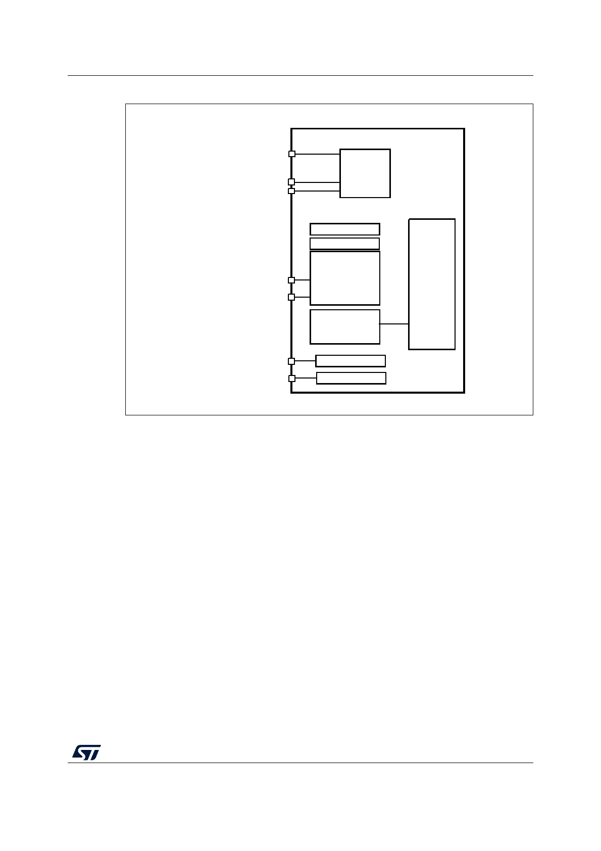
Figure 10. Power supply overview
1. V
DDA
and V
SSA
must be connected to V
DD
and V
SS
, respectively.
2. Depending on the operating power supply range used, some peripherals may be used with limited features
or performance.
3. V
REF+
is only available on TFBGA64 package.
6.1.1 Independent A/D and DAC converter supply and reference voltage
To improve conversion accuracy, the ADC and the DAC have an independent power supply
that can be filtered separately, and shielded from noise on the PCB.
• The ADC voltage supply input is available on a separate V
DDA
pin
• An isolated supply ground connection is provided on the V
SSA
pin
On packages with V
REF+
pin
To ensure a better accuracy on low-voltage inputs and outputs, the user can connect to
V
REF+
a separate external reference voltage lower than V
DD
. V
REF+
is the highest voltage,
represented by the full scale value, for an analog input (ADC) or output (DAC) signal.
For DAC:
1.8 V ≤ V
REF+
≤ V
DDA
For ADC:
1.65 V
≤ V
REF+
< V
DDA
On packages without V
REF+
pin
V
REF+
pin is not available. It is internally connected to the ADC voltage supply (V
DDA
).
MS32791V2
ADC
VDD
VLCD
VSS
IO supply
(VDD) VDDA
(from 1.65 V up to VDDA) VREF+
Te m p . s e n s o r
Reset block
Standby circuitry
(Wakeup logic,
IWDG, RTC,
LSE crystal
32K osc.,
RCC, CSR)
PLL
Voltage regulator
Dynamic voltage
scaling
VDDA domain
DAC
Flash memory
LCD
VDD domain
VCore domain
VDD_USB
USB transceiver
Core
Memories
Digital
peripherals
(VSS) VSSA