RM0367 Rev 7 245/1043
RM0367 General-purpose I/Os (GPIO)
254
Figure 25 shows the alternate function configuration of the I/O port bit.
Figure 25. Alternate function configuration
9.3.12 Analog configuration
When the I/O port is programmed as analog configuration:
• The output buffer is disabled
• The Schmitt trigger input is deactivated, providing zero consumption for every analog
value of the I/O pin. The output of the Schmitt trigger is forced to a constant value (0).
• The weak pull-up and pull-down resistors are disabled by hardware
• Read access to the input data register gets the value “0”
For code example, refer to A.5.3: Analog GPIO configuration code example.
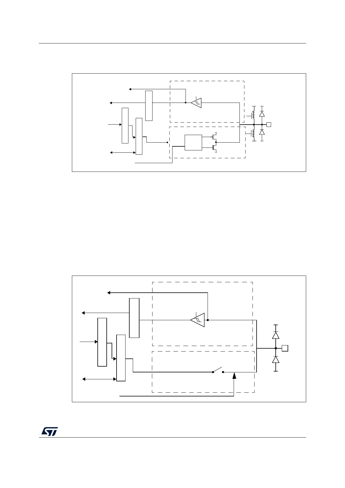
Figure 26 shows the high-impedance, analog-input configuration of the I/O port bits.
Figure 26. High impedance-analog configuration
MSv34756V1
Alternate function output
Alternate function input
push-pull or
open-drain
From on-chip
peripheral
To on-chip
peripheral
Output
control
V
DD
V
SS
TTL Schmitt
trigger
on
Input driver
Output driver
P-MOS
N-MOS
Input data register
Output data register
Read/write
Read
Bit set/reset registers
Write
on/off
on/off
VDDIOx
V
SS
V
SS
protection
diode
protection
diode
Pull
Pull
I/O pin
down
up
VDDIOx
From on-chip
peripheral
To on-chip
peripheral
Analog
trigger
off
Input driver
0
Input data register
Output data register
Read/write
Read
Bit set/reset registers
Write
Analog
V
SS
V
DDIOx
protection
diode
protection
diode
I/O pin
MS31480V1
TTL Schmitt