AES hardware accelerator (AES) RM0367
454/1043 RM0367 Rev 7
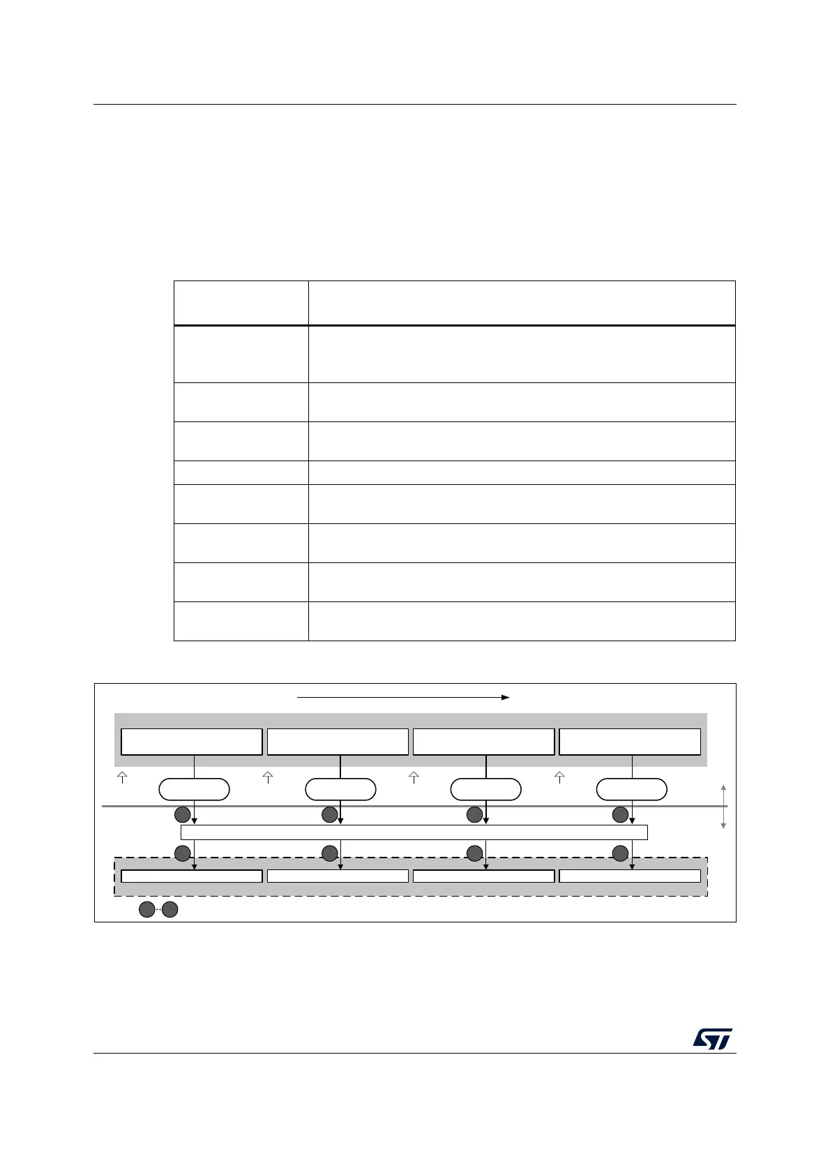
Data input using DMA
Setting the DMAINEN bit of the AES_CR register enables DMA writing into AES. The AES
peripheral then initiates a DMA request during the input phase each time it requires a word
to be written to the AES_DINR register. It asserts four DMA requests to transfer one 128-bit
(four-word) input data block from memory, as shown in Figure 101.
See Table 90 for recommended DMA configuration.
Figure 101. DMA transfer of a 128-bit data block during input phase
Data output using DMA
Setting the DMAOUTEN bit of the AES_CR register enables DMA reading from AES. The
AES peripheral then initiates a DMA request during the Output phase each time it requires a
Table 90. DMA channel configuration for memory-to-AES data transfer
DMA channel control
register field
Recommended configuration
Transfer size
Message length: a multiple of 128 bits.
According to the algorithm and the mode selected, special padding/
ciphertext stealing might be required.
Source burst size
(memory)
Single
Destination burst size
(peripheral)
Single
DMA FIFO size AES FIFO_size = 4 bytes.
Source transfer width
(memory)
32-bit words
Destination transfer
width (peripheral)
32-bit words
Source address
increment (memory)
Yes, after each 32-bit transfer
Destination address
increment (peripheral)
Fixed address of AES_DINR (no increment)
MSv42160V1
AES core input buffer
AES_DINR
LSB
MSB
(No swapping)
Memory accessed through DMA
Word2Word3 Word0Word1
DMA
single write
DMA req N DMA req N+1 DMA req N+2 DMA req N+3
I127 I96
I63 I32
I31 I0
I64I95
D127 D96
D63 D32
D31 D0
D64D95
DIN[127:96] DIN[95:64] DIN[63:32] DIN[31:0]
DMA
single write
DMA
single write
DMA
single write
Chronological order
Increasing address
LSBMSB
AES
peripheral
System
1 2 3 4
1
Order of write to AES_DINR
1 2 3 4
4
 Loading...


