Analog-to-digital converter (ADC) RM0367
304/1043 RM0367 Rev 7
14.3 ADC functional description
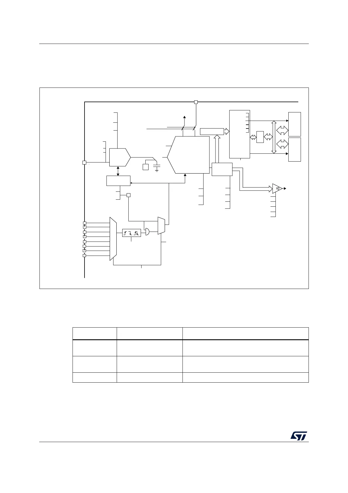
Figure 31 shows the ADC block diagram and Table 58 gives the ADC pin description.
Figure 31. ADC block diagram
1. Refer to Table 60: External triggers for TRGi mapping.
14.3.1 ADC pins and internal signals
MSv33702V7
AHB
to
APB
DMA
CPU
V
REFINT
V
SENSE
LCD_
VLCD1
TRG0
TRG1
TRG2
TRG3
TRG4
SAR ADC
start
master
AHB
ADC V
REF+
1.65 to 3.6 V
SCANDIR up/
down
CH_SEL[18:0]
CONT single/
cont.
ADC_IN[15:0]
V
IN[x]
Input
selection
& scan
control
SMP[2:0]
sampling time
AUTDLY
Auto-delayed conv.
ADSTP
ADSTART
S/W trigger
ADCAL self-
calibration
H/W
trigger
DISCEN
discontinuous
mode
EXTEN[1:0]
trigger enable
and edge selection
EXTSEL[2:0]
trigger selection
RSE[1:0]
12, 10, 8, 6 bits
OVRMOD
overrun mode
ALIGN left/right
Converted data
VIN
Supply and
reference
ADEN/ADDIS
Analog supply
1.8 to 3.6 V
AUTOFF auto-off
mode
AREADY
EOSMP
EOS
EOC
OVR
AWD
DMAEN
DMACFG
DMA request
ADC interrupt
slave
master
IRQ
APB
interface
AWDCHx[4:0]
LTx[11:0]
HTx[11:0]
AWDxSGL
AWDxEN
Analog
watchdog
AWDx
DATA[15:0]
TRG5
TRG6
TRG7
TRGi mapped at
product level
Start & Stop
control
Over-
sampler
TOVS
OVSS[3:0]
OVSR[2:0]
OVSE
Table 58. ADC input/output pins
Name Signal type Remarks
VDDA
Input, analog power
supply
Analog power supply and positive reference voltage
for the ADC
VSSA
Input, analog supply
ground
Ground for analog power supply. Must be at V
SS
potential
ADC_INx Analog input signals 16 external analog input channels