RM0367 Rev 7 861/1043
RM0367 Low-power universal asynchronous receiver transmitter (LPUART)
872
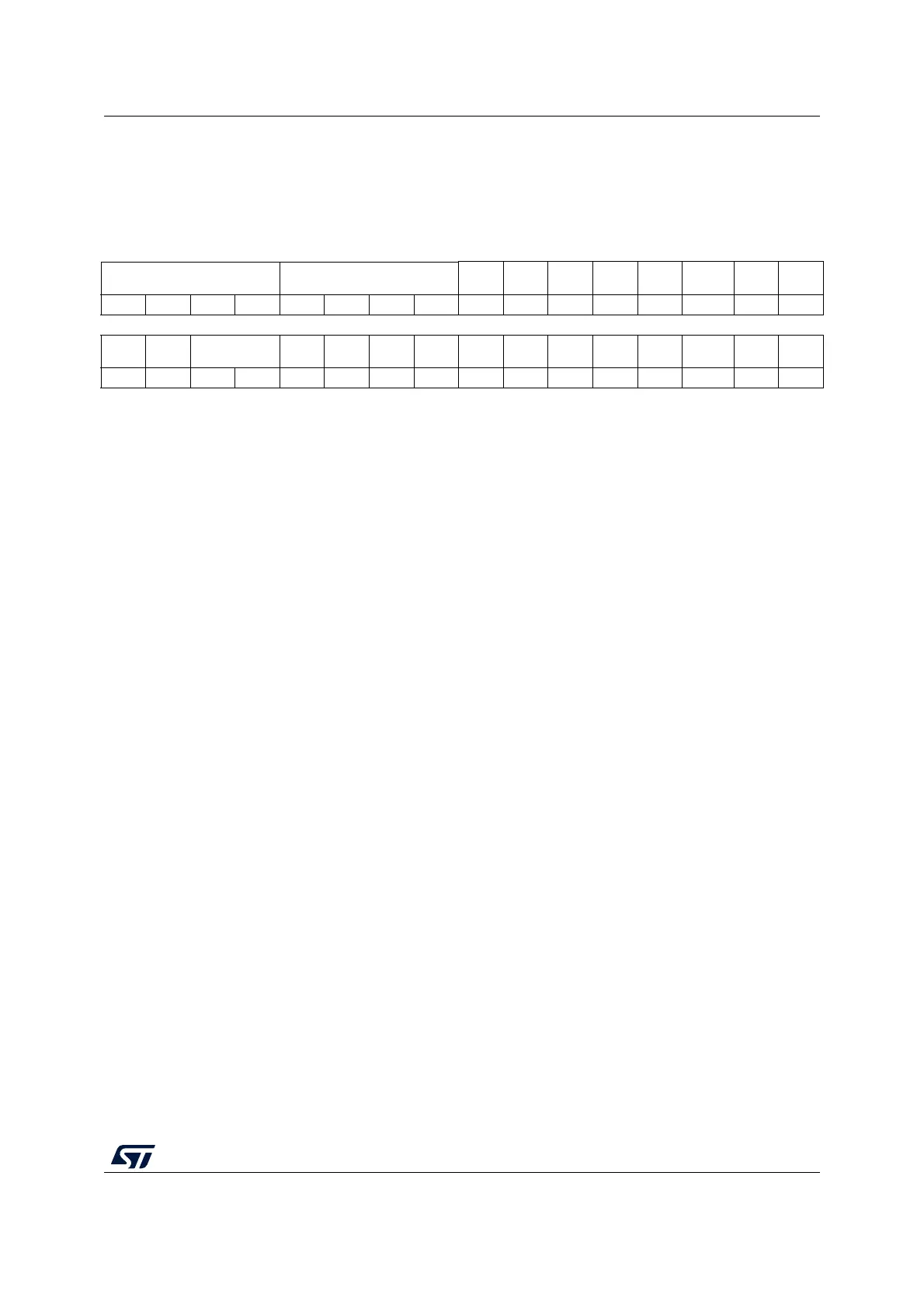
30.7.2 Control register 2 (LPUART_CR2)
Address offset: 0x04
Reset value: 0x0000
31 30 29 28 27 26 25 24 23 22 21 20 19 18 17 16
ADD[7:4] ADD[3:0] Res. Res. Res. Res.
MSBFI
RST
DATAINV TXINV RXINV
rw rw rw rw rw rw rw rw rw rw rw rw
1514131211109876543 2 10
SWAP Res. STOP[1:0] Res. Res. Res. Res. Res. Res. Res. ADDM7 Res. Res. Res. Res.
rw rw rw rw
Bits 31:28 ADD[7:4]: Address of the LPUART node
This bit-field gives the address of the LPUART node or a character code to be recognized.
This is used in multiprocessor communication during Mute mode or Stop mode, for wakeup with 7-
bit address mark detection. The MSB of the character sent by the transmitter should be equal to 1.
It may also be used for character detection during normal reception, Mute mode inactive (for
example, end of block detection in Modbus protocol). In this case, the whole received character (8-
bit) is compared to the ADD[7:0] value and CMF flag is set on match.
This bit field can only be written when reception is disabled (RE = 0) or the LPUART is disabled
(UE=0)
Bits 27:24 ADD[3:0]: Address of the LPUART node
This bit-field gives the address of the LPUART node or a character code to be recognized.
This is used in multiprocessor communication during Mute mode or Stop mode, for wakeup with
address mark detection.
This bit field can only be written when reception is disabled (RE = 0) or the LPUART is disabled
(UE=0)
Bits 23:20 Reserved, must be kept at reset value
Bit 19 MSBFIRST: Most significant bit first
This bit is set and cleared by software.
0: data is transmitted/received with data bit 0 first, following the start bit.
1: data is transmitted/received with the MSB (bit 7/8/9) first, following the start bit.
This bit field can only be written when the LPUART is disabled (UE=0).
Bit 18 DATAINV: Binary data inversion
This bit is set and cleared by software.
0: Logical data from the data register are send/received in positive/direct logic. (1=H, 0=L)
1: Logical data from the data register are send/received in negative/inverse logic. (1=L, 0=H). The
parity bit is also inverted.
This bit field can only be written when the LPUART is disabled (UE=0).
Bit 17 TXINV: TX pin active level inversion
This bit is set and cleared by software.
0: TX pin signal works using the standard logic levels (V
DD
=1/idle, Gnd=0/mark)
1: TX pin signal values are inverted. (V
DD
=0/mark, Gnd=1/idle).
This allows the use of an external inverter on the TX line.
This bit field can only be written when the LPUART is disabled (UE=0).
 Loading...


