09/03
6-64
DC 3535/2240/1632, WC M24
762-xxx Developer NVM List
Initial issue
General Procedures and Information
762-061 AC Bias normal test value 0 0~100 AC Voltage test value at normal speed
762-062 AC Bias normal frequency 60 0~127 AC Voltage frequency at normal speed
762-064 #YM_DB AC Half-speed Frequency 60 0~127 AC Energized Voltage Frequency at YM Color Half Speed
762-065 YM_DB AC Half-speed Output Phase
value
65 0~127 AC Energized Voltage Phase Value at YM Color Half Speed
762-070 #CK_DB AC Half-speed Frequency 60 0~127 AC Energized Voltage Frequency at CK Color Half Speed
762-071 #CK_DB AC Half-speed Output Phase
value
65 0~127 AC Energized Voltage Phase Value at CK Color Half Speed
762-073 #Y_DB DC Vm0 On Normal Timing 110 0~255
1bit=2.4462 msec
Rise timing from 0V to Vm0 for Y Color Normal Speed.
762-074 #M_DB DC Vm0 On Normal Timing 110 0~255
1bit=2.4462 msec
Rise timing from 0V to Vm0 for M Color Normal Speed.
762-075 #C_DB DC Vm0 On Normal Timing 110 0~255
1bit=2.4462 msec
Rise timing from 0V to Vm0 for C Color Normal Speed.
762-076 #K_DB DC Vm0 On Normal Timing 110 0~255
1bit=2.4462 msec
Rise timing from 0V to Vm0 for K Color Normal Speed.
762-077 #Y_DB DC Vm1 Off Normal Timing 90 0~255
1bit=2.4462 msec
Fall timing from Vm1 to Vm0 for Y Color Normal Speed.
762-078 #M_DB DC Vm1 Off Normal Timing 90 0~255
1bit=2.4462 msec
Fall timing from Vm1 to Vm0 for M Color Normal Speed.
762-079 #C_DB DC Vm1 Off Normal Timing 90 0~255
1bit=2.4462 msec
Fall timing from Vm1 to Vm0 for C Color Normal Speed.
762-080 #K_DB DC Vm1 Off Normal Timing 82 0~255
1bit=2.4462msec
Fall timing from Vm1 to Vm0 for K Color Normal Speed.
762-081 #Y_DB DC VB1 On Normal Timing 110 0~255
1bit=2.4462 msec
Rise timing from Vm1 to VB1 for Y Color Normal Speed.
762-082 #M_DB DC VB1 On Normal Timing 110 0~255
1bit=2.4462 msec
Rise timing from Vm1 to VB1 for M Color Normal Speed.
762-083 #C_DB DC VB1 On Normal Timing 110 0~255 Rise timing from Vm1 to VB1 for C Color Normal Speed. (1bit=2.4462 msec.)
762-084 #K_DB DC VB1 On Normal Timing 102 0~255 Rise timing from Vm1 to VB1 for K Color Normal Speed. (1bit=2.4462 msec.)
762-089 #Y_DB DC VB Off Normal Timing 90 0~255 Fall timing from VB to VB2 for Y Color Normal Speed. (1bit=2.4462 msec.)
762-090 #M_DB DC VB Off Normal Timing 90 0~255 Fall timing from VB to VB2 for M Color Normal Speed. (1bit=2.4462 msec.)
762-091 #C_DB DC VB Off Normal Timing 90 0~255 Fall timing from VB to VB2 for C Color Normal Speed. (1bit=2.4462 msec.)
762-092 #K_DB DC VB Off Normal Timing 82 0~255 Fall timing from VB to VB2 for K Color Normal Speed. (1bit=2.4462 msec.)
762-093 #YM_DB AC On Normal Timing 110 0~255 AC Voltage Energized timing for YM Color Normal Speed. (1bit=2.4462 msec.)
762-094 #CK_DB AC On Normal Timing 110 0~255 AC Voltage Energized timing for CK Color Normal Speed. (1bit=2.4462 msec.)
762-095 #YM_DB AC Off Normal Timing 118 0~255 AC Voltage off timing for YM Color Normal Speed. (1bit=2.4462 msec.)
762-096 #CK_DB AC Off Normal Timing 118 0~255 AC Voltage Off timing for CK Color Normal Speed.
762-097 #Y_DB DC Vm0 On half speed timing 104 0~255 Rise timing from 0V to Vm0 for Y Color half speed. (1bit=4.8924 msec.)
762-098 #M_DB DC Vm0 On half speed timing 104 0~255 Rise timing from 0V to Vm0 for M Color half speed. (1bit=4.8924 msec.)
762-099 #C_DB DC Vm0 On half speed timing 104 0~255 Rise timing from 0V to Vm0 for C Color half speed. (1bit=4.8924 msec.)
762-100 #K_DB DC Vm0 On half speed timing 96 0~255 Rise timing from 0V to Vm0 for K Color half speed. (1bit=4.8924 msec.)
762-101 #Y_DB DC Vm1 Off half speed timing 92 0~255 Fall timing from Vm1 to Vm0 for Y Color half speed. (1bit=4.8924 msec.)
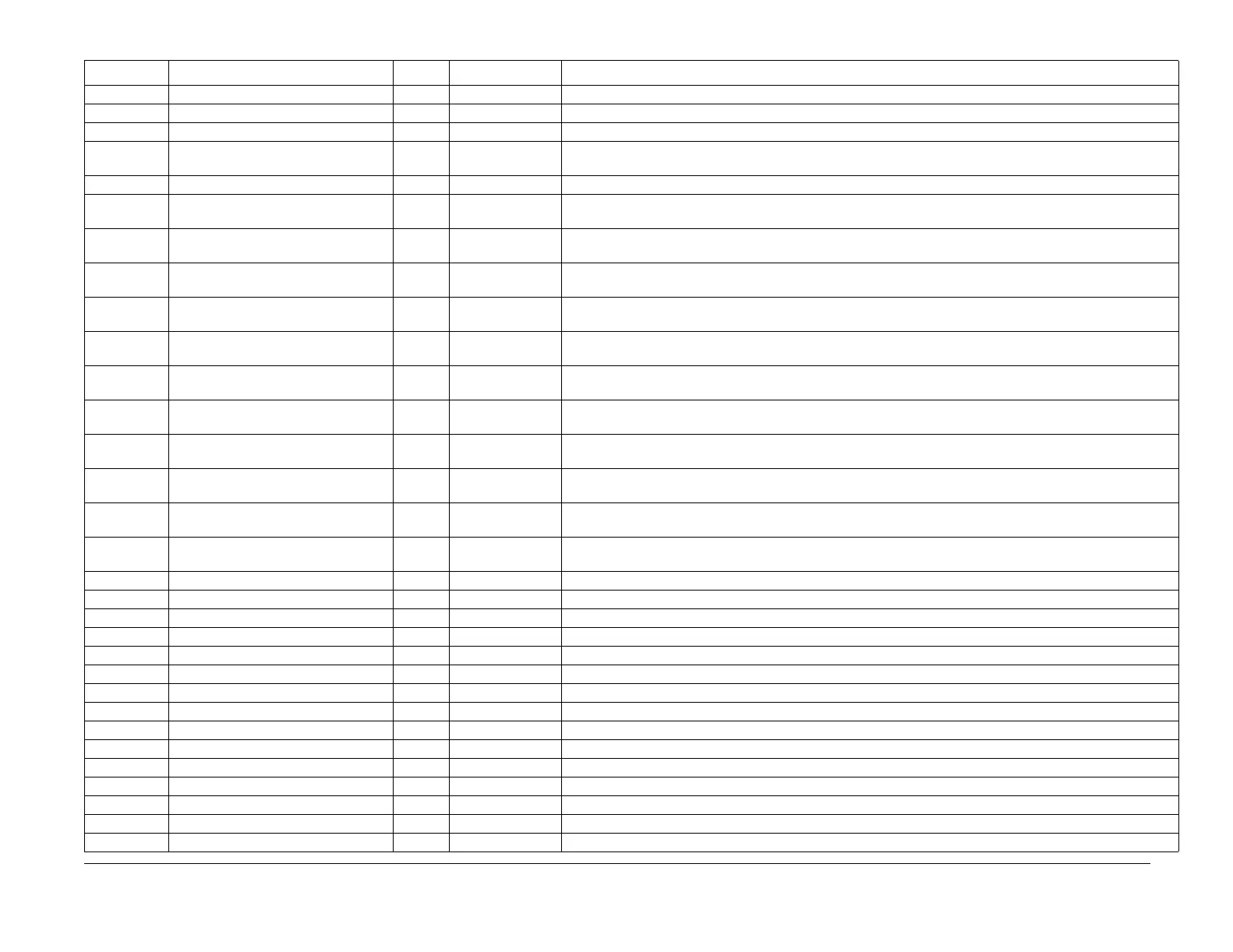
Table 1 Chain 762
Chain-Link Name Default Range Description

 Loading...