Annexes
R&S
®
ZNB/ZNBT
1552User Manual 1173.9163.02 ─ 62
The timing of the data port signals and the input/output signals is as follows:
●
The low pulse of the /WRITE STROBE signal occurs approx. 0.1 μs after a value is
written to the output ports A to D. The pulse duration of the /WRITE STROBE sig-
nal is 1 μs.
●
The low pulse of the /OUTPUT 1 or /OUTPUT 2 signals (if enabled) occur approx.
0.6 μs after the falling edge of the /INPUT 1 signal.
12.3.5 RFFE - GPIO interface
For the R&S ZNB/ZNBT, an optional RFFE GPIO interface board is available.
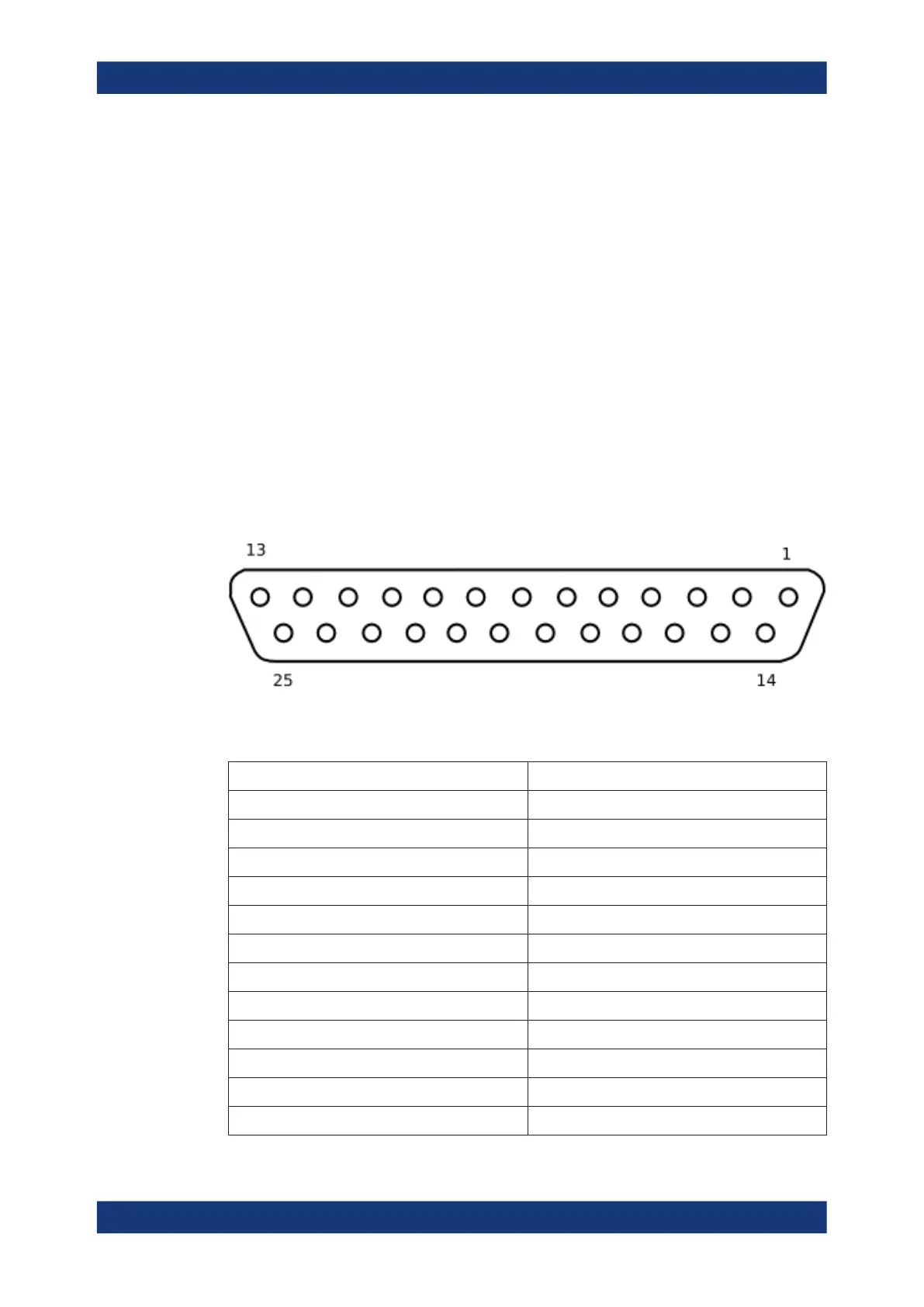
12.3.5.1 Pin assignment
This extension board is equipped with a standard 25-pin female D-sub connector pro-
viding 2 independent RF Front-End (RFFE) interfaces according to the MIPI® Alliance
"System Power Management Interface Specification" and 10 General Purpose Input/
Output (GPIO) ports.
Figure 12-9: D-sub 25-pin female connector, front view
Table 12-2: PIN mapping RFFE - GPIO extension board connector
PIN number Comment
1,3,5,11,22 Ground
2 RFFE1_VIO
4 RFFE2_VIO
6 GPIO 2
7 GPIO 4
8 GPIO 6
9 GPIO 8
10 GPIO 9
12 For future use, please do not connect
13 For future use, please do not connect
14 RFFE1_CLK
15 RFFE1_DATA
Interfaces and connectors
 Loading...