Annexes
R&S
®
ZNB/ZNBT
1548User Manual 1173.9163.02 ─ 62
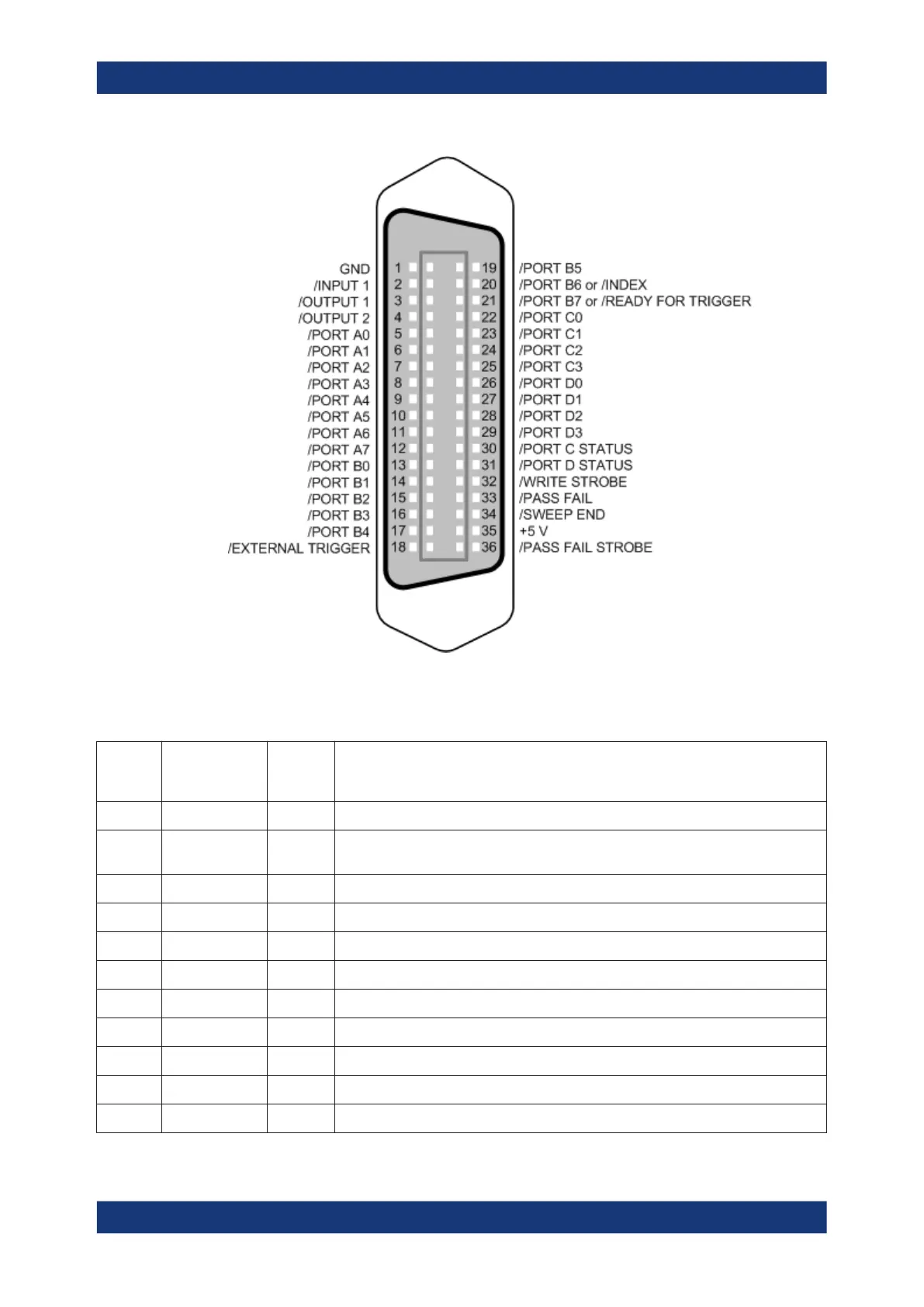
Figure 12-5: Pin assignment of the Universal Interface connector
The input and output signals at the connector are described below.
Pin No. Signal Input (I)
or Out-
put (O)
Description
1 GND – Ground
2 /INPUT 1 I When a negative pulse is fed to this port, the /OUTPUT 1 and /OUTPUT 2 signals (pins
no. 3 and 4) change to "Low".
3 /OUTPUT 1 O Changes to "Low" when the /INPUT 1 (pin no. 2) receives a negative pulse.
4 /OUTPUT 2 O Changes to "Low" when the /INPUT 1 (pin no. 2) receives a negative pulse.
5 /PORT A0 I or O Port A, bit no. 0 (8-bit parallel input or output port)
6 /PORT A1 I or O Port A, bit no. 1
7 /PORT A2 I or O Port A, bit no. 2
8 /PORT A3 I or O Port A, bit no. 3
9 /PORT A4 I or O Port A, bit no. 4
10 /PORT A5 I or O Port A, bit no. 5
11 /PORT A6 I or O Port A, bit no. 6
Interfaces and connectors
 Loading...