Annexes
R&S
®
ZNB/ZNBT
1550User Manual 1173.9163.02 ─ 62
Pin No. Signal Input (I)
or Out-
put (O)
Description
35 +5 V DC O DC power supply for external devices; +5 V ± 250 mV, max. 0.1 A
36 /PASS FAIL
STROBE
O Changes to "Low" when limit check results are present on /PASS FAIL (pin no. 33).
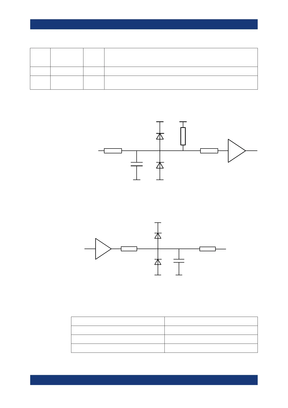
All digital input signals must be TTL compatible with an allowed input voltage range
between –0.5 V and +5.5 V. The circuit diagram of the input path is shown below.
1 k
100
10 k
10 pF
From
Universal
Interface
+5 V +5 V
Figure 12-6: Circuit diagram of the input path
Digital output signals are low-voltage TTL compatible with output voltages between 0 V
and +5 V. The circuit diagram of the output path is shown below.
To
Universal
Interface
100
+5 V
22 pF
10
Figure 12-7: Circuit diagram of the output path
The default configuration of the signals is listed below. Notice that *RST or "Preset" do
not change the configuration of the Universal Interface. Use CONTrol:HANDler:
RESet to restore default values.
Signal *RST Configuration
Port A, Port B Output ports, all bits "High" (decimal 0)
Port C, Port D Input ports
/PORT C STATUS, /PORT D STATUS "Low"
Interfaces and connectors
 Loading...