EPSON AcuLaser CX11/CX11F Revision B
APPENDIX System Connection Diagram 565
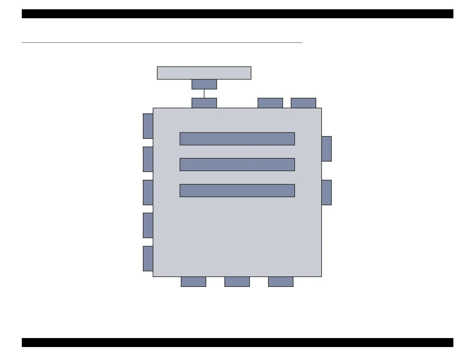
7.1 System Connection Diagram
The following diagram shows the connection between the main board and each system.
Figure 7-1. Main Board Block Diagram
CN704
ADF I/F
*1
(12Pin)
CN705
Sensor I/F
*2
(2Pin)
CN405
Panel I/F
(30Pin)
CN701
CCD_A I/F
(14Pin)
CN702
CCD_B I/F
(13Pin)
CN703
Motor I/F
(4Pin)
Control Panel
CN601
Engine I/F
(16Pin)
CN602
Viedo I/F
(2Pin)
CN300 ROM/RAM DIMM P (90Pin)
CN201 RAM DIMM A (90Pin)
CN202 RAM DIMM B (90Pin)
P
S0
S1
CN502
Power (24V)
(2Pin)
CN410
FAX I/F
*2
(40Pin)
CN402
USB I/F
(2Pin)
CN501
Power (5V, 3.3V)
(2Pin)
CN407
Cobalt I/F
(30Pin)
 Loading...