System Control Coprocessor
ARM DDI 0301H Copyright © 2004-2009 ARM Limited. All rights reserved. 3-7
ID012310 Non-Confidential, Unrestricted Access
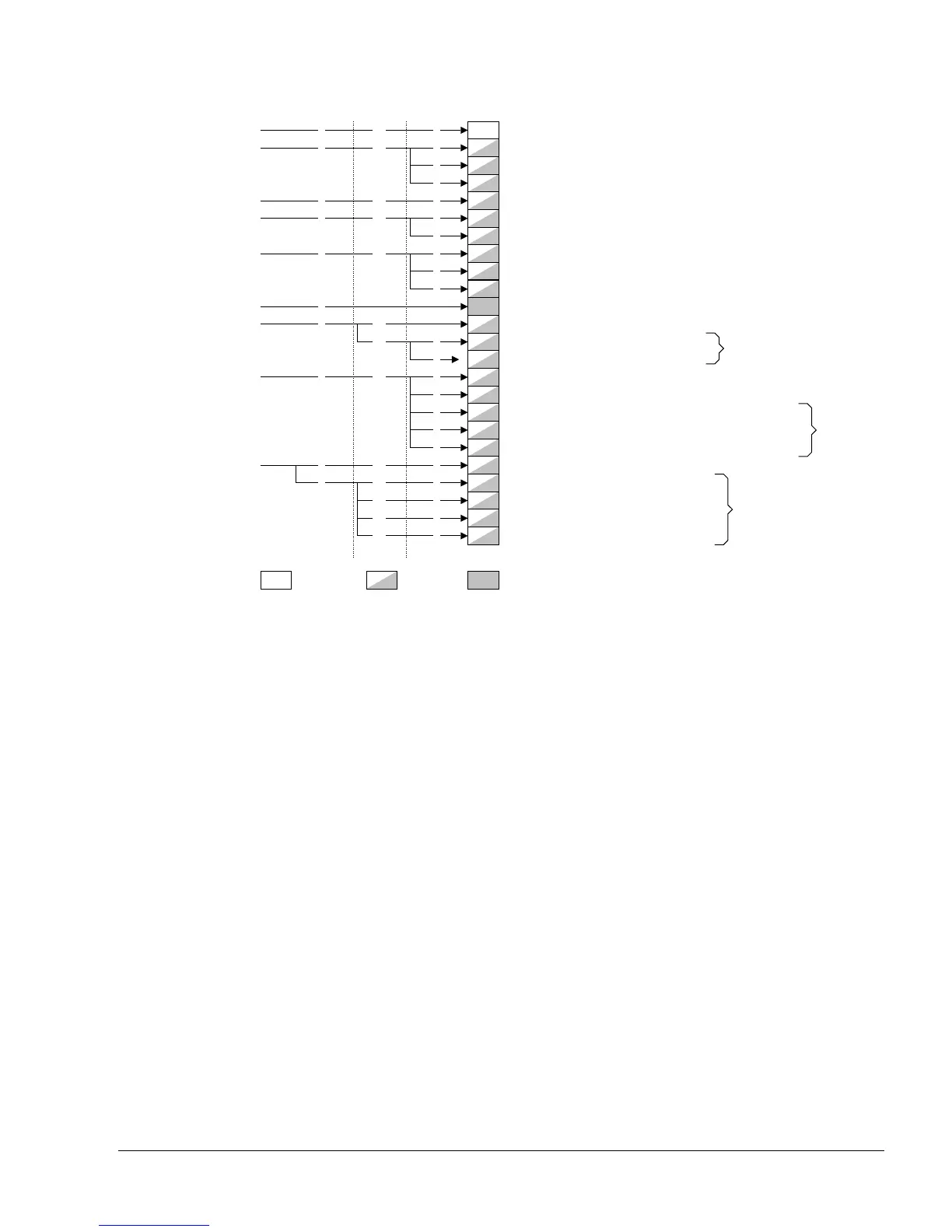
Figure 3-2 MMU control and configuration registers
To use the MMU control and configuration registers you read or write individual registers that
make up the group, see Use of the system control coprocessor on page 3-12.
MMU control and configuration behaves in three ways:
• as a set of numbers, values that describe aspects of the MMU or indicate its current state
• as a set of addresses for tables in memory
• as a set of operations that act on the MMU.
3.1.4 Cache control and configuration
The purpose of the cache control and configuration registers is to:
• provide information on the size and architecture of the instruction and data caches
• control instruction and data cache lockdown
• control cache maintenance operations that include clean and invalidate caches, drain and
flush buffers, and address translation
• override cache behavior during debug or interruptible cache operations.
The cache control and configuration registers consist of one 32-bit read only register and four
32-bit read/write registers. Figure 3-3 on page 3-8 shows the arrangement of the registers in this
functional group.
c0
3
c00
c2
1
2
0
c00
c5
1
0
c00
c6
1
0
c00
c8
0
c10
c3
0
c00
0
c15
2
4
0 c2
c0
TLB Type Register
Translation Table Base Control Register
Translation Table Base Register 1
Translation Table Base Register 0
Instruction Fault Status Register
Data Fault Status Register
Watchpoint Fault Address Register
Fault Address Register
TLB Operations Register
TLB Lockdown Register
Domain Access Control Register
TLB Lockdown Index Register
Peripheral Port Memory Remap Register
Write-onlyRead-only Read/write
CRn CRmOpcode_1
Opcode_2
c13
0
4
c0 FCSE PID Register
Context ID Register
0
2
Instruction Fault Address Register
1
Normal Memory Remap Register
0
c2 Primary Region Remap Register
3
2
1
User Read/Write Thread and Process ID Register
User Read Only Thread and Process ID Register
Privileged Only Thread and Process ID Register
2
5 c4
c5 TLB Lockdown VA Register
2
c6 TLB Lockdown PA Register
2
c7 TLB Lockdown Attributes Register
Memory region
remap registers
Thread and
process ID
registers
TLB lockdown
access registers
Accessible in User mode
 Loading...

