Clocking and Resets
ARM DDI 0301H Copyright © 2004-2009 ARM Limited. All rights reserved. 9-4
ID012310 Non-Confidential, Unrestricted Access
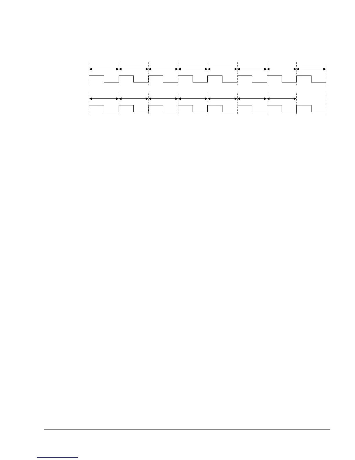
started on the AXI. In the next cycle data is returned to the AXI interface, from where it is
returned first to the level one clock domain before being forwarded to the core. Figure 9-2 shows
this.
Figure 9-2 Read latency with no IEM
The same sequence appears on the I-Side, except that there is less to do in the equivalent RAW
cycle.
9.2.2 Reset with no IEM
The processor has the following reset inputs:
nRESETIN The nRESETIN signal is the main processor reset that initializes the
majority of the processor logic.
DBGnTRST The DBGnTRST signal is the DBGTAP reset.
nPORESETIN The nPORESETIN signal is the power-on reset that initializes the CP14
debug logic. See CP14 registers reset on page 13-25 for details.
nVFPRESETIN The nVFPRESETIN signal is the reset for the VFP block.
All of these are active LOW signals that reset logic in the processor.
The following reset signals are only used if IEM is implemented. Otherwise, these inputs are not
connected to any logic internally, and you must connect them according to your design rules:
• ARESETIn
• ARESETRWn
• ARESETPn
• ARESETDn.
DC1 DC2 RAW L2Req ARVALIDRW RDATARW Data to L1 Data to LSU
Fe1 Fe2 L2Req ARVALIDI RDATAI Data to L1 Data to PU
 Loading...

