Clocking and Resets
ARM DDI 0301H Copyright © 2004-2009 ARM Limited. All rights reserved. 9-6
ID012310 Non-Confidential, Unrestricted Access
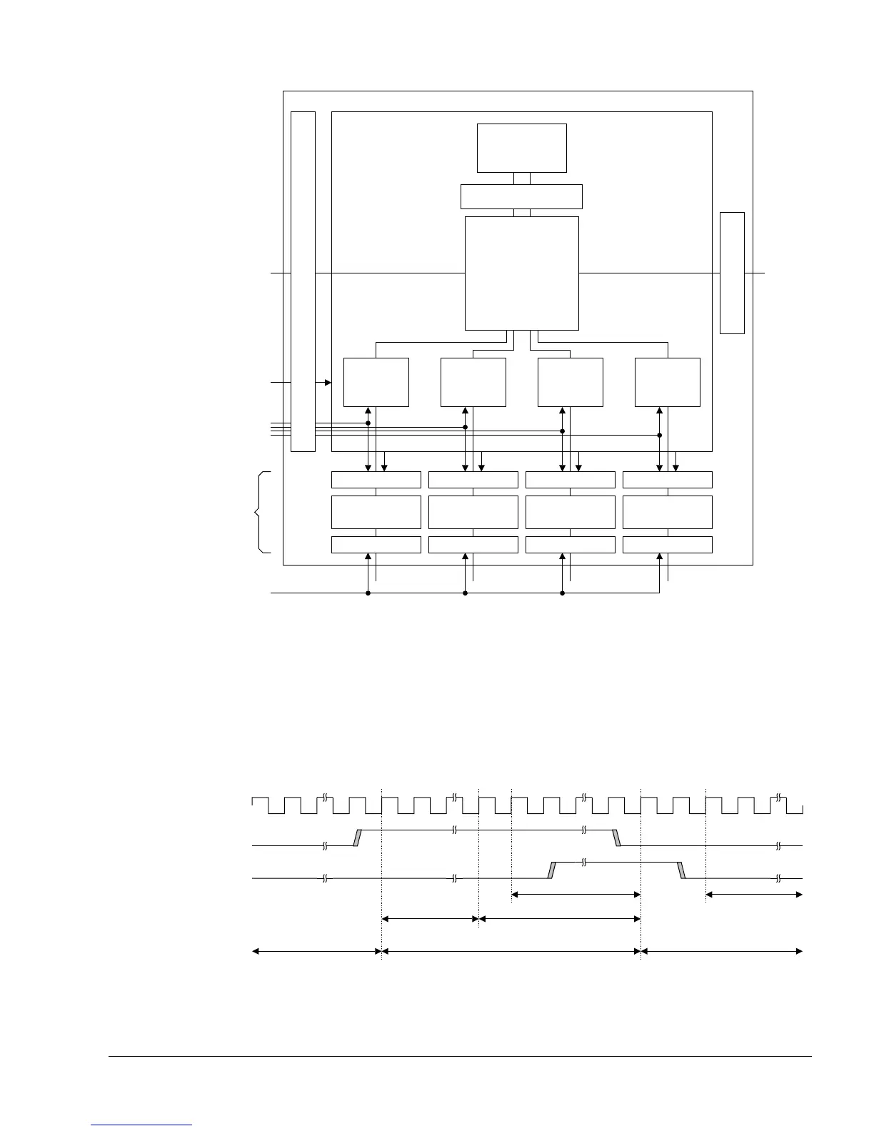
Figure 9-3 Processor clocks with IEM
Synchronization with IEM
When the core runs at maximum performance, the two clocks for the IEM Register Slice are
synchronous. At this point, when frequency and voltage changes have taken effect, the IEM
Register Slice can be bypassed. This removes all the latency that the synchronizers introduce.
The synchronization interface is a simple request and acknowledge system. Figure 9-4 shows
the processor synchronization with such a system.
Figure 9-4 Processor synchronization with IEM
RAMs
Level shift and clamp
Core
Instruction
level 2
interface
DMA level
2 interface
Level shift and clamp
Processor
Clock enables
CLKIN
ACLK clocks
VIC interface
Debug
interface
VCoreSliceI
Data read/
write level
2 interface
Peripheral
level 2
interface
Level shift and clamp
CLK
Level 2
Level shift and
clamp
VSoCSliceI
VCoreSliceRW
Level shift and
clamp
VSoCSliceRW
VCoreSliceD
Level shift and
clamp
VSoCSliceD
VCoreSliceP
Level shift and
clamp
VSoCSliceP
CLK CLK CLK
IEM
register
slices
Clock
SYNCMODEREQ
SYNCMODEACK
FIFO multiplexed out
FIFOs drain
Normal FIFO operation FIFOs closed to new data Normal FIFO operation
Synchronization
over
FIFOs all empty
 Loading...

