Clocking and Resets
ARM DDI 0301H Copyright © 2004-2009 ARM Limited. All rights reserved. 9-3
ID012310 Non-Confidential, Unrestricted Access
9.2 Clocking and resets with no IEM
This section describes clocking and resets for the processor with no IEM:
• Processor clocking with no IEM
• Reset with no IEM on page 9-4.
9.2.1 Processor clocking with no IEM
Externally to the processor, you must connect CLKIN and FREECLKIN together.
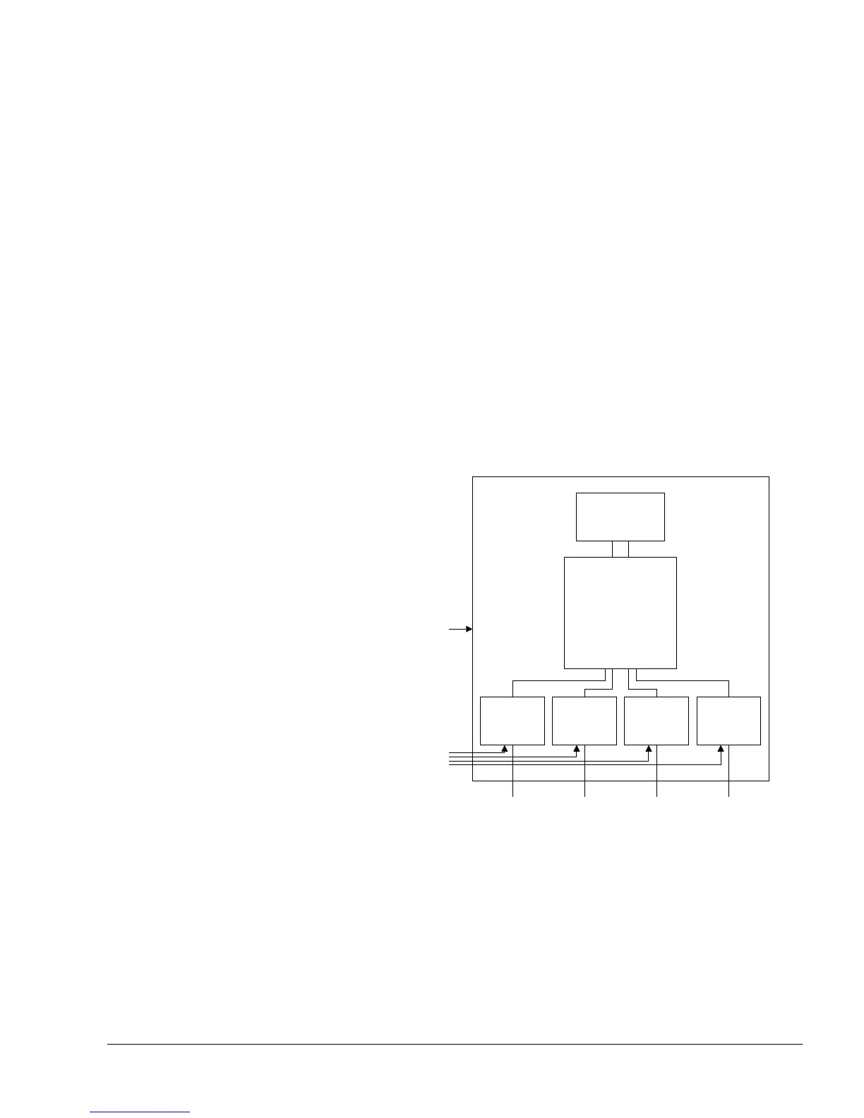
Logically, the processor has only one clock domain.
The four level two interfaces use dedicated clock enables ACLKENI, ACLKENRW,
ACLKENP, and ACLKEND.
The four clock inputs ACLKI, ACLKRW, ACLKP and ACLKD are not used and must be left
unconnected when you implement the processor.
The SYNCMODEREQ* and SYNCMODEACK* signals are not used and must be left
unconnected.
All clocks can be stopped indefinitely without loss of state.
Figure 9-1 shows the clocks for the processor with no IEM.
Figure 9-1 Processor clocks with no IEM
Read latency penalty with no IEM
The Nonsequential Noncacheable read-latency with zero-wait-state AXI is a six-cycle penalty
over a cache hit, where data is returned in the DC2 cycle, on the data side, and a five-cycle
penalty over a cache hit on the instruction side.
In the first cycle after the data cache miss, a read-after-write hazard check is performed against
the contents of the Write Buffer. This prevents stalling while waiting for the Write Buffer to
drain. Following that, a request is made to the AXI interface, and subsequently a transfer is
RAMs
Core
Instruction
level 2
interface
DMA level
2 interface
Clock enables
CLKIN
Data read/
write level
2 interface
Peripheral
level 2
interface
Level 2
 Loading...

