System Control Coprocessor
ARM DDI 0301H Copyright © 2004-2009 ARM Limited. All rights reserved. 3-88
ID012310 Non-Confidential, Unrestricted Access
There are two cache lockdown registers:
• one Data Cache Lockdown Register
• one Instruction Cache Lockdown Register.
The cache lockdown registers are:
•in CP15 c9
• two 32-bit read/write registers, common to the Secure and Non-secure worlds
• accessible in privileged modes only.
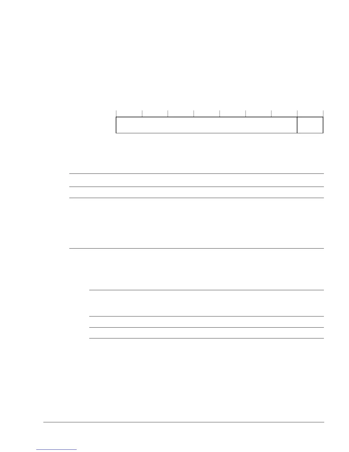
Figure 3-49 shows the bit arrangement of the cache lockdown registers.
Figure 3-49 Instruction and data cache lockdown register formats
Table 3-83 lists how the bit values correspond with the cache lockdown registers functions.
The lockdown behavior depends on the CL bit, see c1, Non-Secure Access Control Register on
page 3-55. If the CL bit is not set, the Lockdown entries are reserved for the Secure world.
Table 3-84 lists the results of attempted access for each mode.
The Data Cache Lockdown Register only supports the Format C method of lockdown. This
method is a cache way based scheme that gives a traditional lockdown function to lock critical
regions in the cache.
A locking bit for each cache way determines if the normal cache allocation mechanisms,
Random or Round-Robin, can access that cache way. For details of the RR bit, that controls the
selection of Random or Round-Robin cache policy, see c1, Control Register on page 3-44.
ARM1176JZF-S processors have an associativity of 4. With all ways locked, the
ARM1176JZF-S processor behaves as if only ways 3 to 1 are locked and way 0 is unlocked.
SBO
31 43 0
L bit for
each cache
way
Table 3-83 Instruction and data cache lockdown register bit functions
Bits Field name Function
[31:4] SBO UNP on reads, SBO on writes.
[3:0] L bit for each
cache way
Locks each cache way individually. The L bits for cache ways 3 to 0 are bits [3:0] respectively.
On a line fill to the cache, data is allocated to unlocked cache ways as determined by the
standard replacement algorithm. Data is not allocated to locked cache ways. If a cache way is
not implemented, then the L bit for that way is hardwired to 1, and writes to that bit are ignored.
0 indicates that this cache way is not locked. Allocation to this cache way is determined by the
standard replacement algorithm. This is the reset state.
1 indicates that this cache way is locked. No allocation is performed to this cache way.
Table 3-84 Results of access to the Instruction and Data Cache Lockdown Register
CL bit value
Secure Privileged Non-secure Privileged
User
Read Write Read Write
0 Data Data Undefined exception Undefined exception Undefined exception
1 Data Data Data Data Undefined exception
 Loading...

