Clocking and Resets
ARM DDI 0301H Copyright © 2004-2009 ARM Limited. All rights reserved. 9-8
ID012310 Non-Confidential, Unrestricted Access
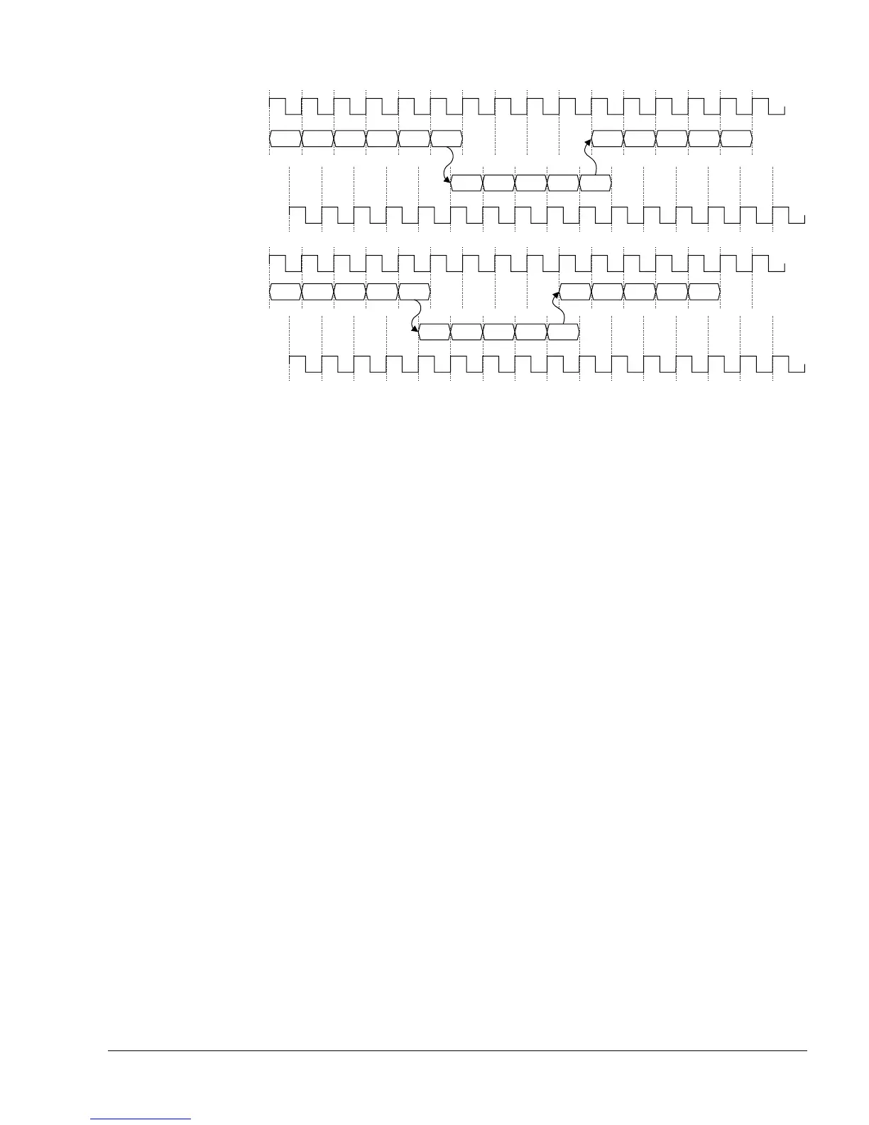
Figure 9-5 Read latency with IEM
The latency, from the pipeline cycles associated with cache reading DC1 and DC2 or Fe1 and
Fe2 to the level two AXI interfaces, is the same as that in Figure 9-2 on page 9-4. The level two
AXI interface, on the Core side of the IEM register slice, asserts ARVALIDRW or ARVALIDI
in cycle AVC. The IEM register slice must then synchronize the address to the ACLK clock
domain on the SoC side. The address is written into an address FIFO in cycle WPA. There are
then two synchronization cycles in the ACLK clock domain, SA1 and SA2, and a buffer cycle
before ARVALID is asserted on the SoC side of the IEM register slice in cycle AVS. Read data
returned from the AXI system in cycle RDS passes through the IEM register slice in a similar
way. In the ACLK clock domain, the data is written into a data FIFO in cycle WPD. The data
then synchronizes in the CLKIN clock domain, in cycles SD1 and SD2, and passes through a
buffer cycle before finally passing to the level two interfaces in cycle RDC. When the level two
interfaces of the core receive the data, they then pass it back to the LSU or PU in two cycles, see
Figure 9-2 on page 9-4.
Each of the IEM register slices, except the peripheral port slice, can store multiple items of read
and write data. This means that a burst of data can typically synchronize in fewer cycles than the
same number of individual data items. The number of cycles required to synchronize a burst of
data depends on:
• the length of the burst
• the ratio of the clock frequencies
• the clock that has the higher frequency
• the latency of the AXI system
• if the operation is a read or write.
9.3.2 Reset with IEM
The processor has the following reset inputs:
nRESETIN The nRESETIN signal is the main processor reset that initializes the
majority of the processor logic.
DBGnTRST The DBGnTRST signal is the DBGTAP reset.
nPORESETIN The nPORESETIN signal is the power-on reset that initializes the CP14
debug logic. See CP14 registers reset on page 13-25 for details.
DC1 DC2 RAW L2R AVC WPA
SA1 SA2 AVS RDS WPD
SD1 SD2 RDC L1 LSU
Fe1 Fe2 L2R AVC WPA
SA1 SA2 AVS RDS WPD
SD1 SD2 RDC L1 PU
CLKIN
ACLKRW
CLKIN
ACLKI
Core
SoC
Core
SoC
 Loading...

