MAX32665-MAX32668 User Guide
Maxim Integrated Page 110 of 457
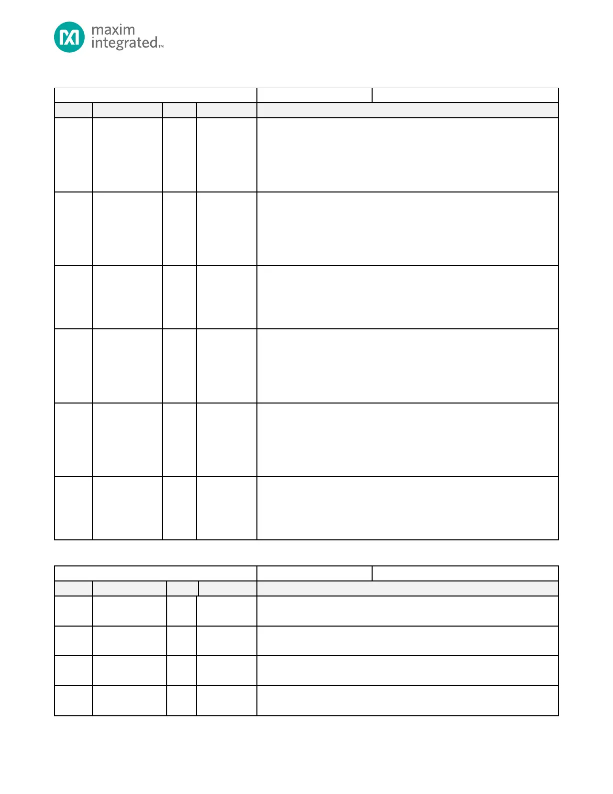
Table 4-71: Error Correction Coding Address Register
Error Correction Coding Address
ECC Error Address/TAG RAM Error
Data depends on which block has reported the error. If sysram, fl0, or fl1, then
this bit(s) represents the bit(s) of the AMBA address of read which produced the
error. If the error is from one of the caches, then this bit is set as shown below:
0: No error
1: Tag_Error. The error is in the TAG RAM
ECC Error Address/TAG RAM Error Bank
Data depends on which block has reported the error. If sysram, fl0, or fl1, then
this bit(s) represents the bit(s) of the AMBA address of read which produced the
error. If the error is from one of the caches, then this bit is set as shown below:
0: Error is in TAG RAM Bank 0
1: Error is in TAG RAM Bank 1
ECC Error Address/TAG RAM Error Address
Data depends on which block has reported the error. If sysram, fl0, or fl1, then
this bit(s) represents the bit(s) of the AMBA address of read which produced the
error. If the error is from one of the caches, then this bit is set as shown below:
[TAG ADDRESS]: Represents the TAG RAM Address
ECC Error Address/DATA RAM Error Address
Data depends on which block has reported the error. If sysram, fl0, or fl1, then
this bit(s) represents the bit(s) of the AMBA address of read which produced the
error. If the error is from one of the caches, then this bit is set as shown below:
0: No error
1: DATA RAM Error. The error is in the Data RAM
ECC Error Address/DATA RAM Error Bank
Data depends on which block has reported the error. If sysram, fl0, or fl1, then
this bit(s) represents the bit(s) of the AMBA address of read which produced the
error. If the error is from one of the caches, then this bit is set as shown below:
0: Error is in DATA RAM Bank 0
1: Error is in DATA RAM Bank 1
ECC Error Address/TAG RAM Error Address
Data depends on which block has reported the error. If sysram, fl0, or fl1, then
this bit(s) represents the bit(s) of the AMBA address of read which produced the
error. If the error is from one of the caches, then this bit is set as shown below:
[DATA ADDRESS]: Represents the DATA RAM Error Address
Table 4-72: Bluetooth LDO Control Register
Reserved
Do not modify this field.
LDOTX Bypass Enable Delay
Not used
LDORX Bypass Enable Delay
Not used.
LDORX Enable Delay
Not used.