MAX32665-MAX32668 User Guide
Maxim Integrated Page 312 of 457
14.4.2 SPI Peripheral Clock
The System Peripheral Clock, PCLK, drives the QSPIn peripheral clock. The SPI0 provides an internal clock, SPI0_CLK, that is
used within the SPI peripheral for the base clock to control the module and generate the SCK clock when in master mode.
Set the SPI0 internal clock using the field QSPIn_CLK_CFG.scale as shown in Equation 14-1. Valid settings for
QSPIn_CLK_CFG.scale are 0 to 8, allowing a divisor of 1 to 256.
Equation 14-1: SPI Peripheral Clock
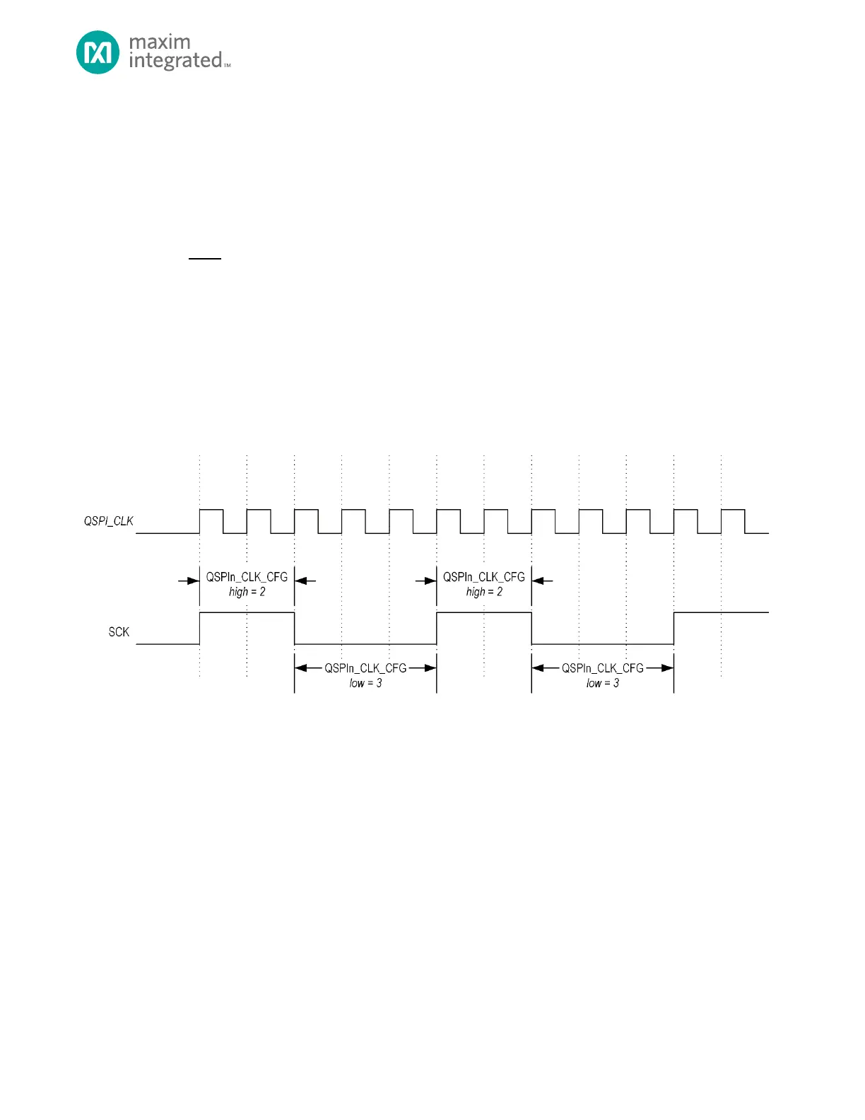
14.4.3 Master Mode Serial Clock Generation
In master and multi-master mode the SCK clock is generated by the master. The SPI0 provides control for both the high
time and low time of the SCK clock. This control allows setting the high and low times for the SCK to duty cycles other than
50% if required. The SCK clock uses the QSPIn peripheral clock as a base value and the high and low values are a count of
the number of
clocks. Figure 14-5, below, visually represents the use of the QSPIn_CLK_CFG.hi and
QSPIn_CLK_CFG.lo fields for a non-50% duty cycle serial clock generation. See Equation 14-2 and Equation 14-3 for
calculating the SCK high and low time from the QSPIn_CLK_CFG.hi and QSPIn_CLK_CFG.lo field values.
Figure 14-5: SCK Clock Rate Control
Equation 14-2: SCK High Time
Equation 14-3: SCK Low Time
14.4.4 Clock Phase and Polarity Control
QSPIn supports four combinations of clock and phase polarity as shown in Table 14-5, below. Clock polarity is controlled
using the bit QSPIn_CTRL2.clkpol and determines if the clock is active high or active low as shown in Figure 14-6. Clock
polarity does not affect the transfer format for SPI. Clock phase determines when the data must be stable for sampling.
Setting the clock phase to 0, QSPIn_CTRL2.phase = 0, dictates the SPI data is sampled on the initial SPI clock edge regardless
of clock polarity. Phase 1, QSPIn_CTRL2.phase = 1, results in data sample occurring on the second edge of the clock
regardless of clock polarity.