MAX32665-MAX32668 User Guide
Maxim Integrated Page 160 of 457
causes the slave select to de-assert. The SPIXF block requires reconfiguration prior to subsequent access to external SPI
flash space either for execution or data reads.
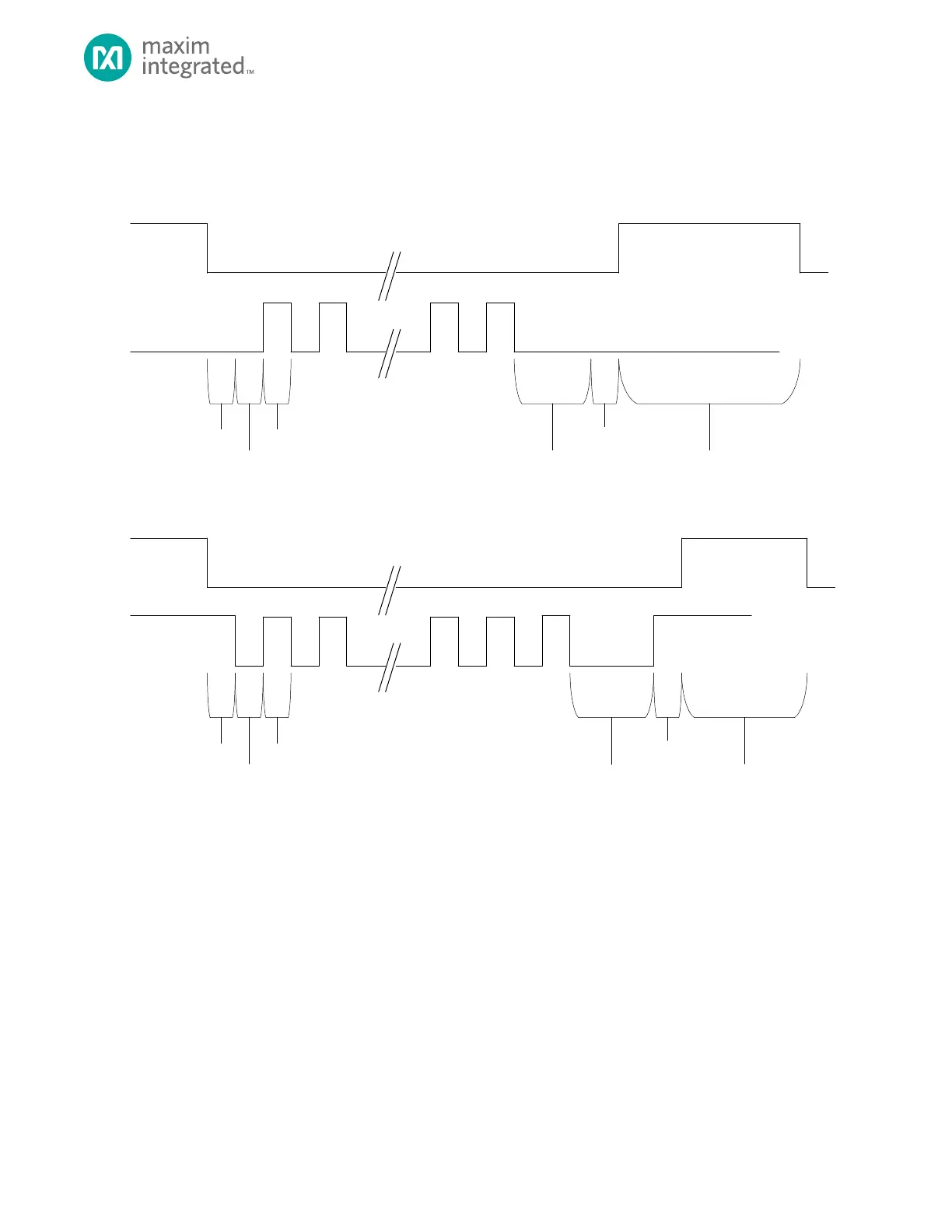
Figure 8-5. SPIXFM Delay Configuration
SPIXFM MODE 0
SPIXFM_CFG.ssact
SPIXFM_CFG.loclk
SPIXFM_CFG.hiclk
SS
SCK
Several clocks (min 3)
delay due to comple tion
of AHB transa ction
SPIXFM_CFG.ssact
SPIXFM_CFG.ssiact
SPIXFM_CFG.ssact
SPIXFM_CFG.loclk
SPIXFM_CFG.hiclk
SS
SCK
SPIXFM_CFG.ssact
SPIXFM_CFG.ssinact
Bit 0
Extra
Pulse
SPIXFM MODE 3
An extra pulse is provided at the end of this transaction to
comply with some SPI fla sh timing diagrams, and allow for
highe r speeds during SPI READ transa ctions.
Several clocks (min 3)
delay due to comple tion
of AHB transa ction
8.2.2.3 SPIXF Read Sequence Configuration and Control
Assertion of SPIXF slave select followed by the read command, then the read address. After the read address is sent 0 or
more clocks are generated (called dummy bytes or mode clocks) to allow the flash to access the data being addressed. The
remainder of the SPI access is read data. Sequential bytes are read until the de-assertion of SPIXF slave select.
Depending on the read command and the SPI flash configuration, the read command is sent over 1, 2, or 4 bits per clock.
The same is true for the address, data, and mode/dummy clocks. Also, configure the device to eliminate the sending of the
read command once the command is sent to the SPI flash device. This is enabled and disabled through special data sent
during the mode or dummy period between address and read data.