MAX32665-MAX32668 User Guide
Maxim Integrated Page 164 of 457
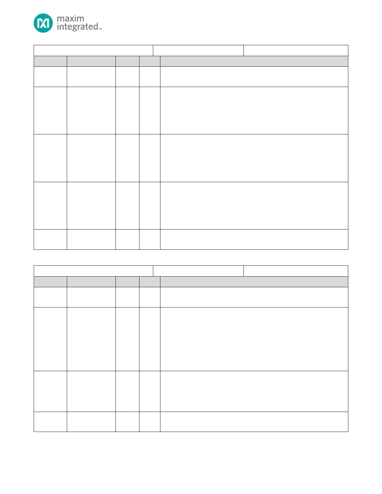
SPIXFM Fetch Control Register
Reserved for Future Use
Do not modify this field.
Data Width
Number of data I/O used to receive data.
0b00: Single SDIO
0b01: Dual SDIO
0b10: Quad SDIO
0b11: Reserved
Address Width
Number of data I/O used to send address and mode/dummy clocks.
0b00: Single SDIO
0b01: Dual SDIO
0b10: Quad SDIO
0b11: Reserved
Command Width
Number of data I/O used to send commands.
0b00: Single SDIO
0b01: Dual SDIO
0b10: Quad SDIO
0b11: Reserved
Command Value
Command value sent to target to initiate fetching from SPI flash.
Table 8-18. SPIXFM Mode Control Register
SPIXFM Mode Control Register
Reserved for Future Use
Do not modify this field.
Mode Send
Setting this field ensures that the next SPI flash transaction will send the mode
byte as defined in the SPIXFM_MODE_DATA.mddata field.
When this field is set, the next SPI flash read operation exits continuous mode
cleanly. This field and the SPIXFM_MODE_CTRL.nocmd field is automatically
cleared by hardware after the next SPI transaction.
0: No Action.
1: Send Mode Byte on next transaction
No Command Mode
Read command sent only once after this bit is set.
0: Send read command every time SPI transaction is initiated.
1: Send read command on first transaction only and not on subsequent
transactions.
Reserved for Future Use
Do not modify this field.