MAX32665-MAX32668 User Guide
Maxim Integrated Page 165 of 457
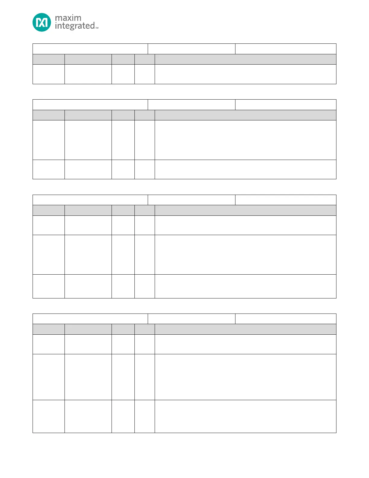
SPIXFM Mode Control Register
Mode Clocks
Number of SPI clocks needed during the mode/dummy phase of fetch.
Table 8-19. SPIXFM Mode Data Register
SPIXFM Mode Data Register
Mode Output Enable
Output enable state for each corresponding data bit in
SPIXFM_MODE_DATA.mddata.
0: Output enable off, I/O is tristate stated.
1: Output enable on, I/O is driving SPIXFM_MODE_DATA.mddata.
Mode Data
Specifies the data to send with the dummy/mode clocks.
Table 8-20. SPIXFM SCK Feedback Control Register
SPIXFM SCK Feedback Control Register
Reserved for Future Use
Do not modify this field.
SCK feedback Clock inversion.
The feedback clock can be phase selected to increase the timing margin for
input data from the slave external flash device.
0: Non-inverted SCK is used for feedback clock
1: Inverted SCK is used for feedback clock
SCK Feedback Mode Enable. Enable SCK feedback mode
0: Disable SCK feedback mode
1: Enable SCK feedback mode
Table 8-21. SPIXFM I/O Control Register
SPIXFM I/O Control Register
Reserved for Future Use
Do not modify this field.
IO Pullup/Pulldown Control
These bits control the pullups and pulldowns associated with all SPIXF SDIO pins.
0b00: tristate
0b01: pullup
0b10: pulldown
0b11: pullup
SDIO Drive Strength
This bit controls the drive strength of all SDIO pins.
0: Low Drive Strength.
1: Hi Drive Strength.