MAX32665-MAX32668 User Guide
Maxim Integrated Page 255 of 457
11.9 Registers
See Table 3-1: APB Peripheral Base Address Map for the base peripheral address of these registers. All fields are reset on
peripheral, system, or power-on reset events unless otherwise specified.
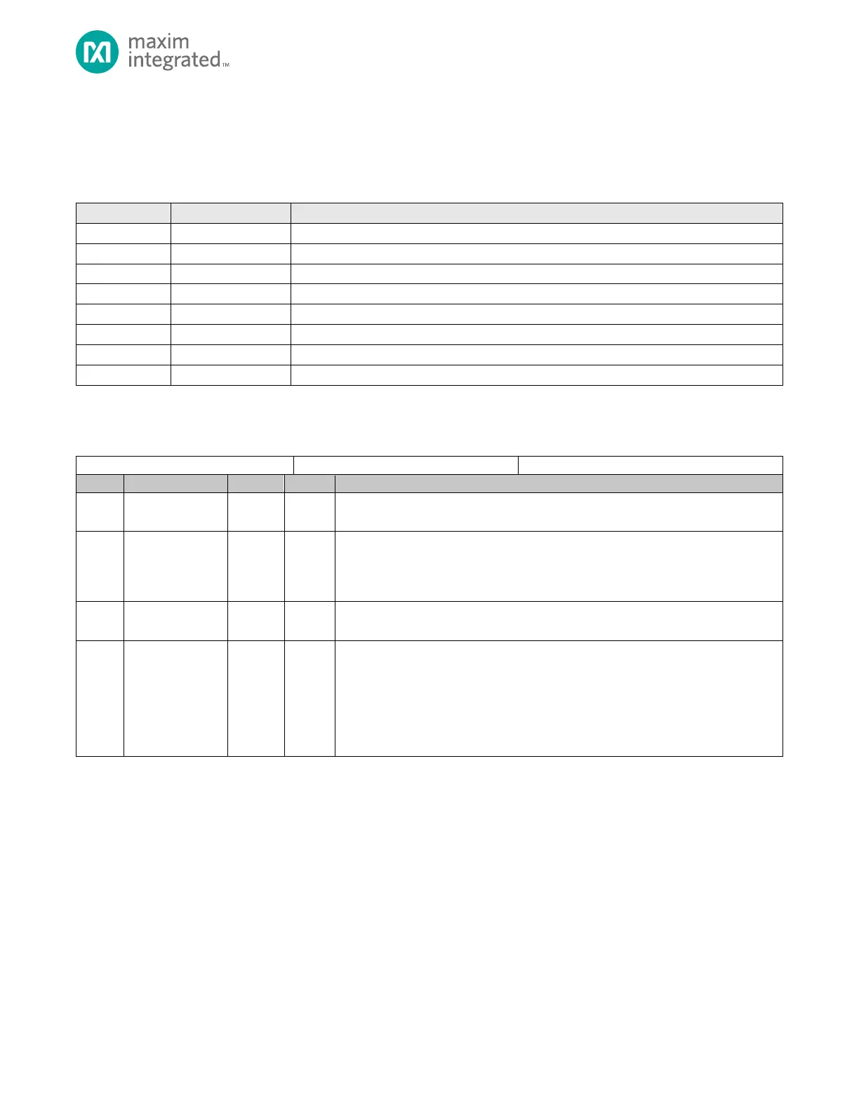
Table 11-5. ADC Registers Summary
ADC Interrupt Control Register
11.10 Register Details
Table 11-6: ADC Control Register
Reserved for Future Use
Do not modify this field.
ADC Data Alignment
Selects the alignment of the 16-bit data conversion stored in the DATA register.
0: Data is LSB justified in 16-bit DATA register. DATA[15:10] = 0.
1: Data is MSB justified in 16-bit DATA register. DATA[5:0] = 0.
Reserved for Future Use
Do not modify this field.
External Input Scale
Scales the external inouts AIN0-AIN7. All eight of external inputs are scaled by the
same value
0x0: No scaling.
0x1: Divide by 2
0x2: Divide by 3
0x3: Divide by 4