MAX32665-MAX32668 User Guide
Maxim Integrated Page 313 of 457
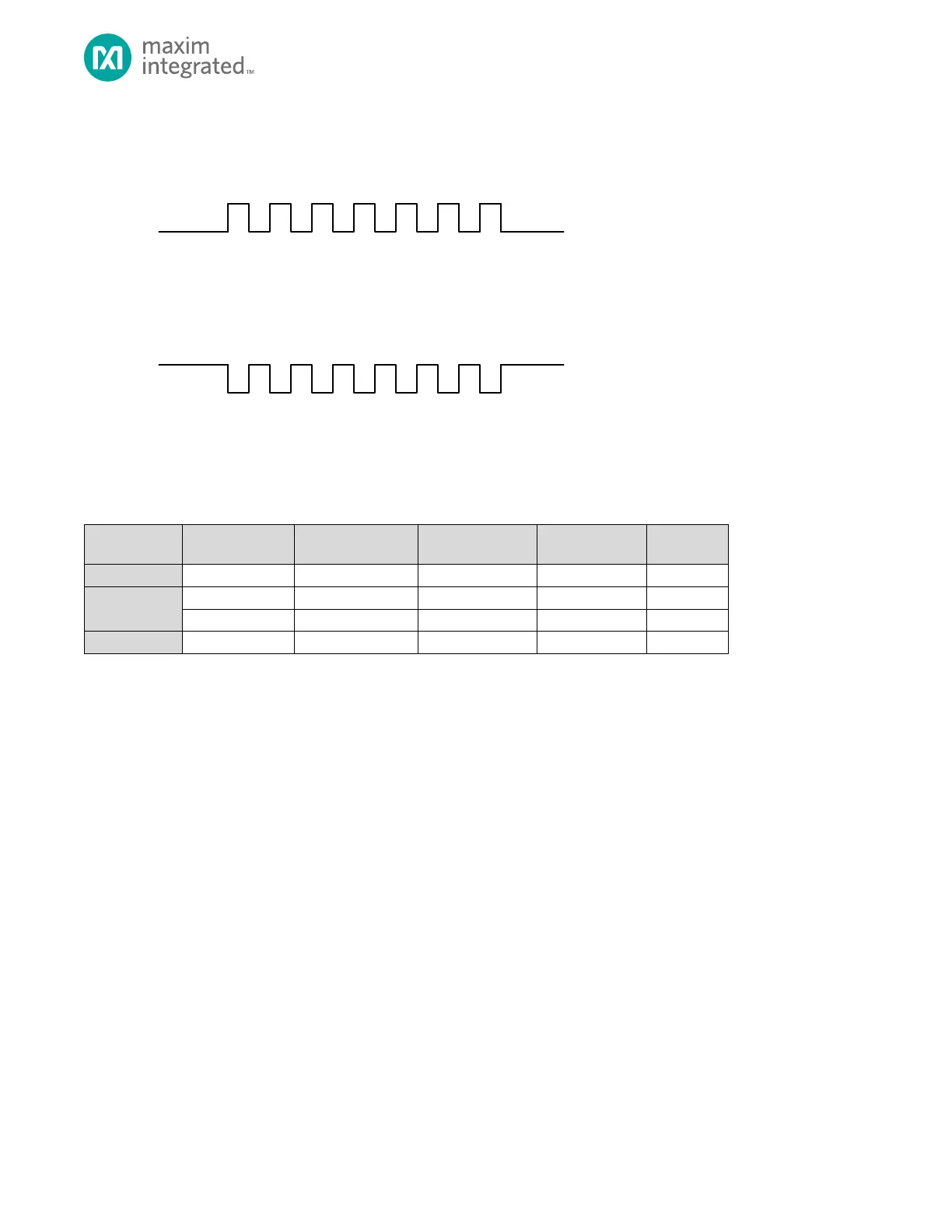
Figure 14-6: SPI Clock Polarity
For proper data transmission, the clock phase and polarity must be identical for the SPI master and slave. The master
always places data on the MOSI line a half-cycle before the SCK edge for the slave to latch the data.
Table 14-5. SPI Modes Clock Phase and Polarity Operation
14.4.5 QSPIn FIFOs
The Transmit FIFO hardware is 32 bytes deep. The write data width can be 8-, 16- or 32-bits wide. A 16-bit write queues a
16-bit word to the FIFO hardware. A 32-bit write queues two 16-bit words to the FIFO hardware with the least significant
word dequeued first. Bytes must be written to two consecutive byte addresses, with the odd byte as the most significant
byte, and the even byte as the least significant byte. The FIFO logic waits for both the odd and even bytes to be written to
this register space before dequeuing the 16-bit result to the FIFO.
The Receive FIFO hardware is 32 bytes deep. Read data width can be 8-, 16- or 32-bits. A byte read from this register
dequeues one byte from the FIFO. A 16-bit read from this register dequeues two bytes from the FIFO, least significant byte
first. A 32-bit read from this register dequeues four bytes from the FIFO, least significant byte first.
14.4.6 QSPI Interrupts and Wakeups
The QSPIn supports multiple interrupt sources. Status flags for each interrupt are set regardless of the state of the interrupt
enable bit for that event. The event happens once when the condition is satisfied. The status flag must be cleared by
firmware by writing a 1 to the interrupt flag.