MAX32665-MAX32668 User Guide
Maxim Integrated Page 240 of 457
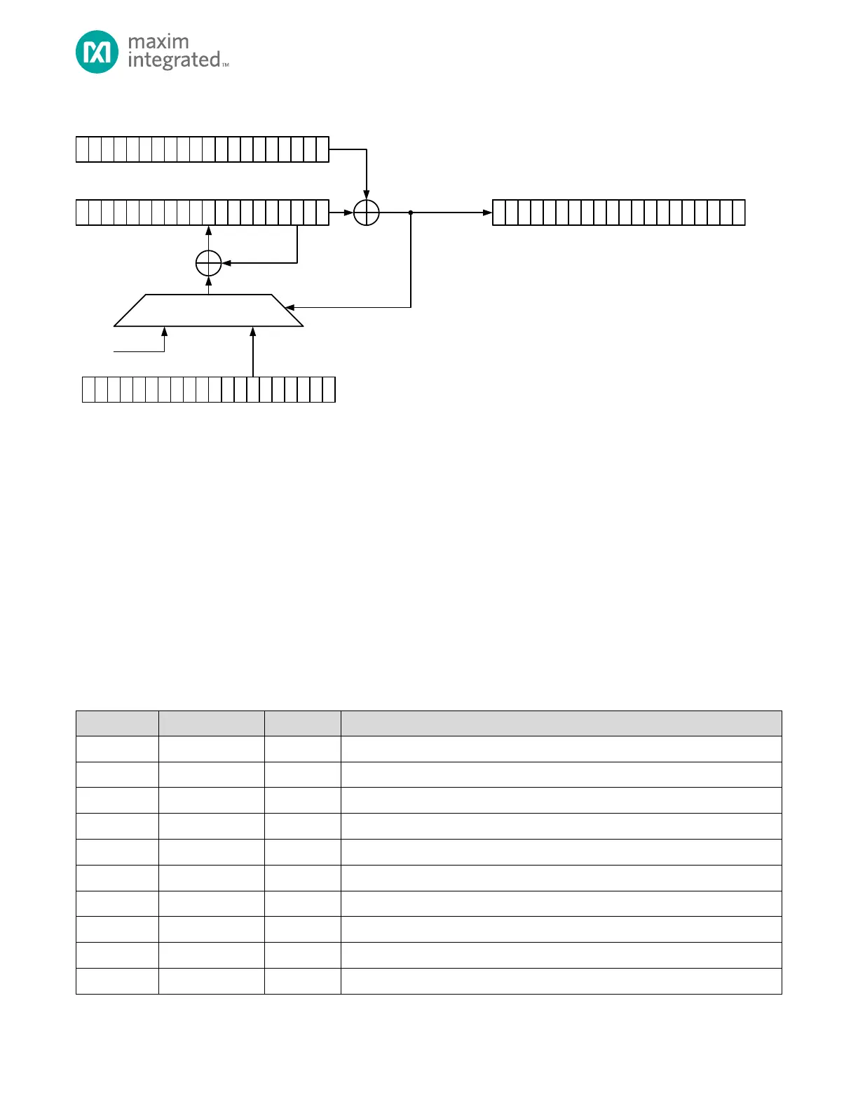
Figure 10-1: Galois Field CRC and LFSR Architecture
Different polynomials generate different sequences of random data. Ideally, an n-bit polynomial generates a random
sequence of
bits. Not all polynomials are maximal length. Some repeat before the theoretical maximum length of
. There are thousands of different maximal length 32-bit LFSR polynomials. You can use any length of an LFSR
polynomial up to 32 bits. Some tables of maximal length LFSR polynomials omit the MSB
term or the LSB
term. Fibonacci LFSRs feed back the XOR of all the taps to the constant term
. It is often implied when listing the taps
but must be present when writing the polynomial to the CRC_POLY register.
The crypto accelerator automatically generates the next sequence of 32 bits whenever the CRYPTO_LFSR register is read. If
the PRNG control bit is set, the incoming data is forced to zero. You can use the DMA to quickly fill a block of memory with
pseudo-random data.
10.3 Registers
See Table 3-1: APB Peripheral Base Address Map for this peripheral/module's base address. If multiple instances are
provided, each will have a unique base address. Unless specified otherwise, all fields are reset on a system reset, soft reset,
POR, and the peripheral-specific reset, if applicable.
Table 10-2: CRC Register Summary