MAX32665-MAX32668 User Guide
Maxim Integrated Page 171 of 457
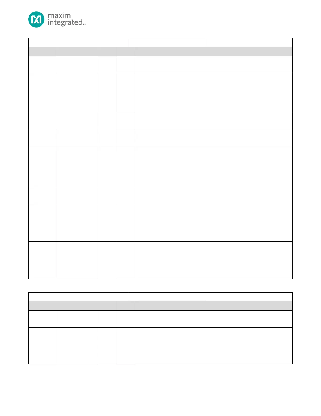
SPIXR Static Configuration Register
Reserved for Future Use
Do not modify this field.
SPIXR Data Width
Sets the number of data lines (SDIO pins) for communication.
0: 1-data pin (Single Mode)
1: 2-data pins (Dual Mode)
2: 4-data pins (Quad Mode)
3: Reserved for Future Use
Number of Bits per Character
Sets the number of bits per character for an SPIXR transaction.
Reserved for Future Use
Do not modify this field.
SCK Inverted
This field must always be set to 0 for SPIXR operation. SCK inversion for a
specific mode is not supported by the SPIXR peripheral. Use the
SPIXR_CTRL3.cpol field to set the polarity of the clock for a given mode.
0: Normal SCK output.
1: Invalid, not supported.
Reserved for Future Use
Do not modify this field.
Clock Polarity
Sets the SCK clock polarity for the supported modes.
0: Normal clock. Use when in SPI Mode 0 and Mode 1
1: Inverted clock. Use when in SPI Mode 2 and Mode 3
Note: This field is set depending on the SPI Mode configuration.
Clock Phase
Sets the SPIXR SCK clock phase.
0: Data sampled on clock rising edge. Use when in SPI Mode 0 and Mode 2
1: Data sampled on clock falling edge. Use when in SPI Mode 1 and Mode 3
Note: This field must be set based on the SPI Mode configuration.
Table 8-29. SPIXR Slave Select Timing Register
SPIXR Slave Select Timing Register
Reserved for Future Use
Do not modify this field.
SS Inactive Clock Delay
This is the time SS is inactive, and the bus is inactive between character
transmission.
It is the number of system clock cycles from the time a character is transmitted,
and SS is inactive to the time SS is active and a new character is transmitted.