MAX32665-MAX32668 User Guide
Maxim Integrated Page 193 of 457
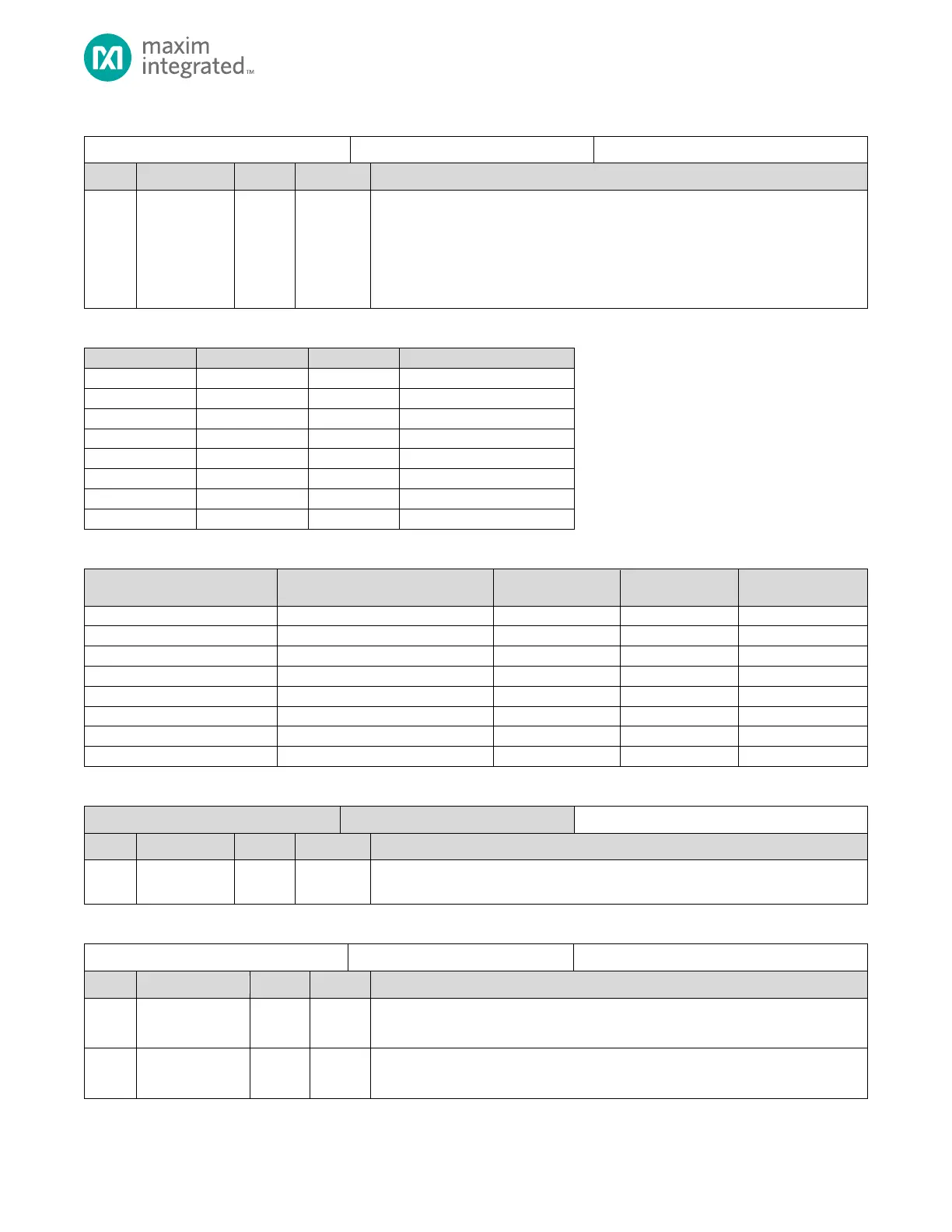
Table 8-61: SDHC Response 7 Register
Response Register 7
Response 7 to Response 0 registers are referenced as a contiguous, single register in
the SD Host Controller Spec V3.0. Table 8-62 shows the mapping from the Response
Registers to the SD Host Controller Standard Specification REP[127:0] notation for the
MAX32665—MAX32668. Table 8-63 shows the SD types of response mapped to the
MAX32665—MAX32668 Response registers.
Table 8-62: SDHC Response Register Mapping to SD Host Controller Response Register Convention
Table 8-63: Kind of SD Card Response Mapping to SDHC Response Registers
REP[] Specification
Mapping
SDHC Response
Register MSW
SDHC Response
Register LSW
R1, R1b (normal response)
R1b (Auto CMD12 response)
Card Status for Auto CMD12
Card Status for Auto CMD23
OCR register for I/O, etc
R6 (Published RCA response)
Newly published RCA[31:16], etc
Table 8-64: SDHC Buffer Data Port Register
Buffer Data Port Register
Buffer Data
Pointer to the SDHC internal data buffer.
Table 8-65: SDHC Present State Register
Reserved for Future Use
Do not modify this field.
CMD Line Signal Level
Indicates the CMD line level for error recovery and debugging.