MAX32665-MAX32668 User Guide
Maxim Integrated Page 83 of 457
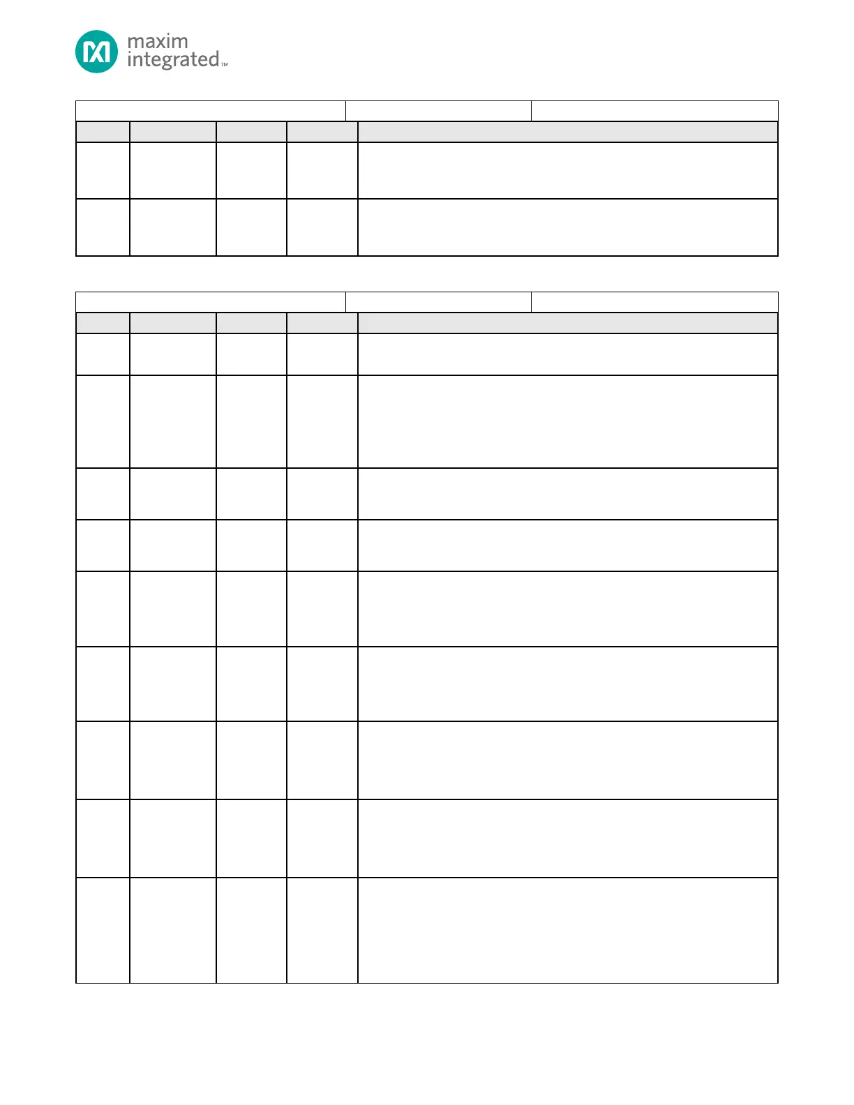
Peripheral Low Power Wakeup Enable
USB VBUS State Change Wakeup Enable
Write 1 to enable an interrupt and wakeup the device from any low power
mode when PWRSEQ_LPPWST.usbvbuswkst = 1.
USB Line State Change Wakeup Enable
Write 0b11 to enable an interrupt and wakeup the device from any low power
mode when PWRSEQ_LPPWST.usblswkst does not equal 0.
Table 4-49: RAM Shutdown Control Register
Reserved
Do not modify this field.
Internal Flash ICC1 Shut Down
Write 1 to shut off power to the Internal Flash Memory ICC1.
Note: When this field is set, the contents of the Internal Flash Memory ICache1
RAM are destroyed. See GCR_MEM_CLK register for retention mode power
settings
ROM1 Shut Down
0: Power enabled.
1: Power shut down.
ROM0 Shut Down
0: Power enabled.
1: Power shut down.
USB FIFO Shut Down
0: Power enabled.
1: Power shut down. Affected memory is destroyed.
Note: See GCR_MEM_CLK register for retention mode power settings.
Crypto MAA RAM Shut Down
0: Power enabled.
1: Power shut down. Affected memory is destroyed.
Note: See GCR_MEM_CLK register for retention mode power settings.
SRCC Cache RAM Shut Down
Write 1 to shut off power to the SPI-XIPR Cache RAM.
Note: When this field is set, the contents of the SPI-XIPR Cache RAM, are
destroyed. See GCR_MEM_CLK register for retention mode power settings.
SFCC Cache RAM Shut Down
Write 1 to shut off power to the SPI-XIPF Cache RAM.
Note: When this field is set, the contents of the SPI-XIPF Cache RAM, are
destroyed. See GCR_MEM_CLK register for retention mode power settings.
Internal Flash ICC0 Shut Down
0: Power enabled.
1: Power shut down. Affected memory is destroyed.
See Table 4-13 RAM Block Size and Base Address for base address and size
information. Note: See GCR_MEM_CLK register for retention mode power
settings.