EasyManuals Logo

Maxim Integrated MAX32665 User Manual

Maxim Integrated MAX32665
457 pages
To Next Page IconTo Next Page
To Previous Page IconTo Previous Page
Page #182 background imageLoading...
Page #182 background image
MAX32665-MAX32668 User Guide
Maxim Integrated Page 182 of 457
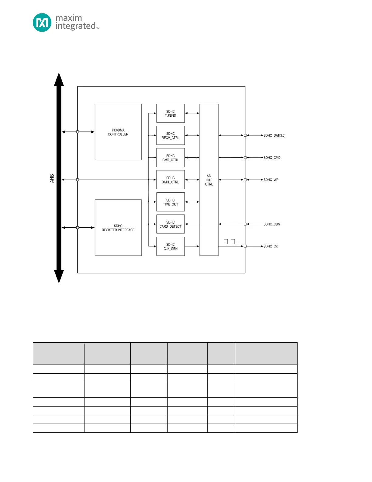
Figure 8-7: SDHC Block Diagram
8.5.1 Instances
The SDHC pin mapping for the SD Host Controller Standard Specification Version 3.0 are shown in Table 8-43, below.
Table 8-43: MAX32665MAX32668 SDHC Alternate Function Mapping to SDHC Specification Pin Names
Alternate Function
Alternate Function
Number
Pin Name
SDHC
Specification
Pin Name
Direction
Signal Description
SDHC_CDN
AF1
P1.7
SDCD#
I
Card present, active low.
SDHC_CLK
AF1
P1.3
SDCLK
O
SD clock signal.
SDHC_WP
AF1
P1.6
SDWP
I
Write protect signal,
active high.
SDHC_CMD
AF1
P1.1
CMD
I/O
SD bus command signal.
SDHC_DAT0
AF1
P1.2
DAT[0]
I/O
SD data bus bit 0.
SDHC_DAT1
AF1
P1.4
DAT[1]
I/O
SD data bus bit 1.
SDHC_DAT2
AF1
P1.5
DAT[2]
I/O
SD data bus bit 2.

Table of Contents

Questions and Answers:

Question and Answer IconNeed help?

Do you have a question about the Maxim Integrated MAX32665 and is the answer not in the manual?

Maxim Integrated MAX32665 Specifications

General IconGeneral
BrandMaxim Integrated
ModelMAX32665
CategoryMotherboard
LanguageEnglish