MAX32665-MAX32668 User Guide
Maxim Integrated Page 244 of 457
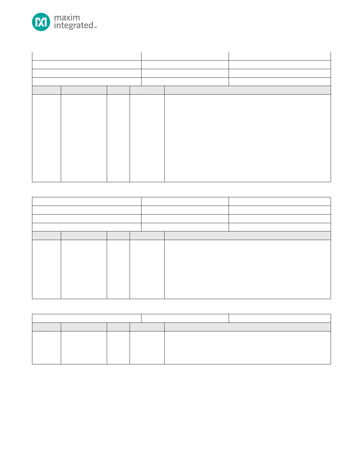
Table 10-7: CRC Data Input Registers
CRC Data Input Register 0
CRC Data Input Register 1
CRC Data Input Register 2
CRC Data Input Register 3
CRC Data Input
Writes to this register bypass the DMA interface and put data directly into
the CRC FIFO. Data written to a register is placed into the FIFO in the order
it is written. CRC_DATA_IN3:CRC_DATA_IN0 represent 128 bits with
CRC_DATA_IN3 mapped to bits 127:96, CRC_DATA_IN2 mapped to bits
95:64, CRC_DATA_IN1 mapped to bits 63:32 and CRC_DATA_IN0 mapped
to bits 31:0.
CRC_DATA_IN3:CRC_DATA_IN0 occupy four successive words to allow the
use of multi-store instructions. Writes to any location are supported and
writes are loaded into the CRC FIFO in the order they are written.
Note: The CRC_DATA_INn registers are affected by the input endian swap
bit, CRYPTO_CTRL.bsi.
Table 10-8: CRC Data Output Registers
CRC Data Output Register 0
CRC Data Output Register 1
CRC Data Output Register 2
CRC Data Output Register 3
CRC Data Output
The output from the CRC is written to the CRC_DATA_OUT3:
CRC_DATA_OUT0 registers representing a total of 128 bits.
CRC_DATA_OUT3 maps to bits 127:96, CRC_DATA_OUT2 maps to bits
95:64, CRC_DATA_OUT1 maps to bits 63:31, and CRC_DATA_OUT0
represents output bits 31:0.
Note: The CRC_DATA_OUTn registers are affected by the output endian
swap bit, CRYPTO_CTRL.bso.
Table 10-9: CRC Polynomial Register
CRC Polynomial
The polynomial used for Galois Field calculations (CRC or LFSR) is written to
this register.
Note: This register is affected by the MSB control bit, CRC_CTRL.msb.