MAX32665-MAX32668 User Guide
Maxim Integrated Page 113 of 457
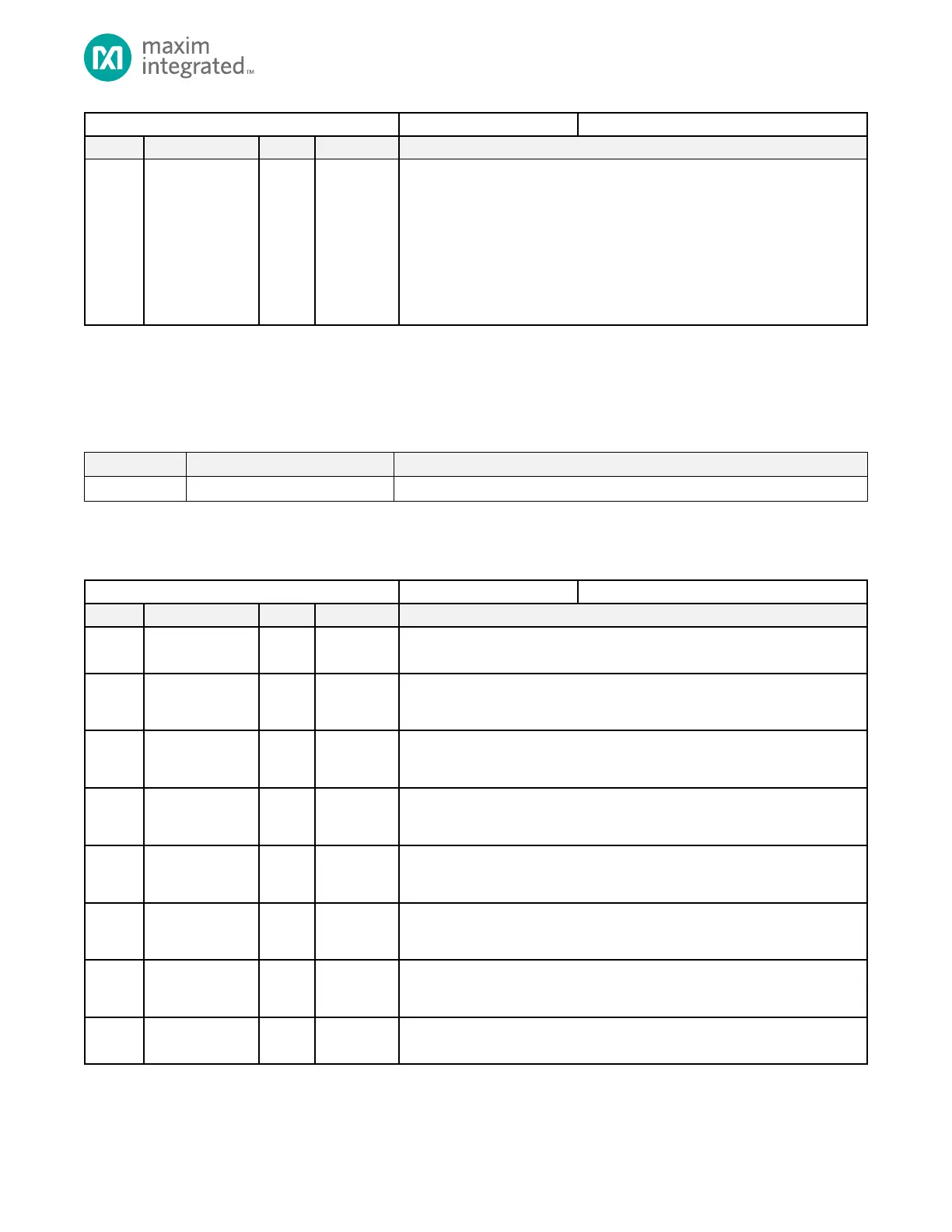
Arm Peripheral Bus Asynchronous Bridge Select
I2C0 Peripheral Bus Select
The access for this peripheral can be performed via one of two different
peripheral bus configurations. The system PCLK can be used as any of the other
system peripherals that are connected to the APB PCLK domain or a 7.3728MHz
bus can be used. It takes 3 cycles of the 7.3728MHz clock to switch PCLK or 3
cycles of the PCLK clock to switch to 7.37MHz clock. After switching, ensure
enough time before accessing the peripheral registers.
0: PCLK bus selected
1: 7.3728MHz bus selected
4.18 Function Control Registers
See Table 3-1: APB Peripheral Base Address Map for this module's base address. Unless specified otherwise, all fields are
reset only on a system reset or POR, but not a soft reset.
Table 4-76: Function Control Register Summary
Function Control Register
4.19 Function Control Register Details
Table 4-77: Function Control Register 0
Reserved
Do not modify this field.
I2C2 SCL Glitch Filter Enable
0: Disabled
1: Enabled
I2C2 SDA Glitch Filter Enable
0: Disabled
1: Enabled
I2C1 SCL Glitch Filter Enable
0: Disabled
1: Enabled
I2C1 SDA Glitch Filter Enable
0: Disabled
1: Enabled
I2C0 SCL Glitch Filter Enable
0: Disabled
1: Enabled
I2C0 SDA Glitch Filter Enable
0: Disabled
1: Enabled
Reserved
Do not modify this field.